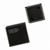
P87C591VFA/00,512 NXP Semiconductors, P87C591VFA/00,512 Datasheet - Page 9

P87C591VFA/00,512
Manufacturer Part Number
P87C591VFA/00,512
Description
IC 80C51 MCU 16K OTP 44-PLCC
Manufacturer
NXP Semiconductors
Series
87Cr
Datasheet
1.P87C591VFA00512.pdf
(160 pages)
Specifications of P87C591VFA/00,512
Core Processor
8051
Core Size
8-Bit
Speed
12MHz
Connectivity
CAN, EBI/EMI, I²C, UART/USART
Peripherals
POR, PWM, WDT
Number Of I /o
32
Program Memory Size
16KB (16K x 8)
Program Memory Type
OTP
Ram Size
512 x 8
Voltage - Supply (vcc/vdd)
4.75 V ~ 5.25 V
Data Converters
A/D 6x10b
Oscillator Type
Internal
Operating Temperature
-40°C ~ 85°C
Package / Case
44-PLCC
Processor Series
P87C5x
Core
80C51
Data Bus Width
8 bit
Data Ram Size
512 B
Interface Type
CAN, I2C, UART
Maximum Clock Frequency
12 MHz
Number Of Programmable I/os
32
Number Of Timers
3
Maximum Operating Temperature
+ 85 C
Mounting Style
SMD/SMT
3rd Party Development Tools
PK51, CA51, A51, ULINK2
Minimum Operating Temperature
- 40 C
On-chip Adc
10 bit, 6 Channel
Lead Free Status / RoHS Status
Lead free / RoHS Compliant
Eeprom Size
-
Lead Free Status / Rohs Status
Details
Other names
568-1256-5
935268182512
P87C591VFAA
935268182512
P87C591VFAA
Available stocks
Company
Part Number
Manufacturer
Quantity
Price
Company:
Part Number:
P87C591VFA/00,512
Manufacturer:
TI
Quantity:
8
Company:
Part Number:
P87C591VFA/00,512
Manufacturer:
NXP Semiconductors
Quantity:
10 000
Philips Semiconductors
6.2
Table 1 Pin description for QFP44/PLCC44, see Note 1.
2000 Jul 26
RST
P3.0to P3.7
P3.0/RXD
P3.1/TXD
P3.2/INT0/CMSR0 8
P3.3/INT1/
CMSR1
P3.4/T0/CMSR2
P3.5/T1/CMSR3
P3.6/WR
P3.7/RD
XTAL2
XTAL1
V
V
SS
DD
Single-chip 8-bit microcontroller with CAN controller
SYMBOL
Pin description
4
5
7
9
10
11
12
13
14
15
16
17
QFP44 PLCC44
PIN
10
11
13
14
15
16
17
18
19
20
21
22
23
Reset: A Input to reset the P8xC591. It also provides a reset pulse as output
when Timer T3 overflows.
Port 3 (P3.0 to P3.7): 8-bit programmable I/O port lines; Port 3 can
sink/source 4 LSTTL inputs.
Port 3 pins serve alternate functions as follows:
RXD: Serial input port for UART;
T2: T2 event input
TXD: Serial output port for UART;
RT2: T2 timer reset signal. Rising edge triggered.
INT0: External interrupt input 0;
CMSR0: Compare and Set/Reset output for Timer T2.
INT1: External interrupt input 1;
CMSR1: Compare and Set/Reset output for Timer T2.
T0: Timer 0 external interrupt input;
CMSR2: Compare and Set/Reset output for Timer T2.
T1: Timer 1 external interrupt input;
CMSR3: Compare and Set/Reset output for Timer T2.
WR: External Data Memory Write strobe;
RD: External Data Memory Read strobe.
During reset, Port 3 will be asynchronously driven resistive HIGH.
Port 3 has four modes selected on a per bit basis by writing to the P3M1 and
P3M2 registers as follows:
P3M1.x
Crystal pin 2: output of the inverting amplifier that forms the oscillator. Left
open-circuit when an external oscillator clock is used.
Crystal pin 1: input to the inverting amplifier that forms the oscillator, and
input to the internal clock generator. Receives the external oscillator clock
signal when an external oscillator is used.
Ground; circuit ground potential.
Power supply; power supply pin during normal operation and power
reduction modes.
0
0
1
1
P3M2.x
0
1
0
1
9
Mode Description
Pseudo-bidirectional (standard c51 configuration default)
Push-Pull
High impedance
Open drain
DESCRIPTION
Preliminary Specification
P8xC591


