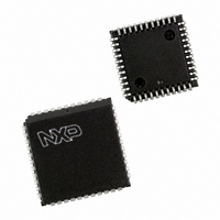
P87C591VFA/00,512 NXP Semiconductors, P87C591VFA/00,512 Datasheet - Page 42

P87C591VFA/00,512
Manufacturer Part Number
P87C591VFA/00,512
Description
IC 80C51 MCU 16K OTP 44-PLCC
Manufacturer
NXP Semiconductors
Series
87Cr
Datasheet
1.P87C591VFA00512.pdf
(160 pages)
Specifications of P87C591VFA/00,512
Core Processor
8051
Core Size
8-Bit
Speed
12MHz
Connectivity
CAN, EBI/EMI, I²C, UART/USART
Peripherals
POR, PWM, WDT
Number Of I /o
32
Program Memory Size
16KB (16K x 8)
Program Memory Type
OTP
Ram Size
512 x 8
Voltage - Supply (vcc/vdd)
4.75 V ~ 5.25 V
Data Converters
A/D 6x10b
Oscillator Type
Internal
Operating Temperature
-40°C ~ 85°C
Package / Case
44-PLCC
Processor Series
P87C5x
Core
80C51
Data Bus Width
8 bit
Data Ram Size
512 B
Interface Type
CAN, I2C, UART
Maximum Clock Frequency
12 MHz
Number Of Programmable I/os
32
Number Of Timers
3
Maximum Operating Temperature
+ 85 C
Mounting Style
SMD/SMT
3rd Party Development Tools
PK51, CA51, A51, ULINK2
Minimum Operating Temperature
- 40 C
On-chip Adc
10 bit, 6 Channel
Lead Free Status / RoHS Status
Lead free / RoHS Compliant
Eeprom Size
-
Lead Free Status / Rohs Status
Details
Other names
568-1256-5
935268182512
P87C591VFAA
935268182512
P87C591VFAA
Available stocks
Company
Part Number
Manufacturer
Quantity
Price
Company:
Part Number:
P87C591VFA/00,512
Manufacturer:
TI
Quantity:
8
Company:
Part Number:
P87C591VFA/00,512
Manufacturer:
NXP Semiconductors
Quantity:
10 000
Philips Semiconductors
12.5.10 RX M
The RMC Register (CAN Address 9) reflects the number of messages available within the RXFIFO. The value is
incremented with each receive event and decremented by the Release Receive Buffer command. After any reset event,
this register is cleared.
Table 22 RX Message Counter (RMC) (CAN address 9)
12.5.11 RX B
The RBSA register (CAN Address 10) reflects the currently
valid internal RAM address, where the first byte of the
received message, which is mapped to the Receive Buffer
Window, is stored. With the help of this information it is
possible to interpret the internal RAM contents. The
internal RAM address area begins at CAN address 32 and
may be accessed by the CPU for reading and writing
(writing in Reset Mode only).
Example:
If RBSA is set to 24 (decimal), the current message visible
in the Receive Buffer Window (CAN Address 96 -108) is
stored within the internal RAM beginning at RAM address
24. Because the RAM is also mapped directly to the CAN
address space beginning at CAN address 128 (equal to
RAM address 0) this message may also be accessed
using CAN address 152 and the following bytes
Table 23 RX Buffer Start Address (RBSA) (CAN address 10)
2000 Jul 26
Single-chip 8-bit microcontroller with CAN controller
RBSA.7
RMC.7
7
7
UFFER
ESSAGE
RBSA.6
RMC.6
6
6
S
TART
C
OUNTER
A
DDRESS
RBSA.5
RMC.5
(RMC)
5
5
(RBSA)
RBSA.4
RMC.4
4
4
42
(CAN Address = RBSA + 128--> 24 + 128= 152).
Always, the Release Receive Buffer Command is given
while there is at least one more message available within
the FIFO, RBSA is updated to the beginning of the next
message.
On Hardware Reset, this pointer is initialised to “00h”.
Upon a Software Reset (setting of Reset Mode) this
pointer keeps its old value, but the FIFO is cleared, what
means, that the RAM contents are not changed, but the
next received (or transmitted) message will override the
currently visible message within the Receive Buffer
Window.
The RX Buffer Start Address Register appears to the CPU
as a read only memory in Operating Mode and as read /
write memory in Reset Mode.
RBSA.3
RMC.3
3
3
RBSA.2
RMC.2
2
2
RBSA.1
RMC.1
Preliminary Specification
1
1
P8xC591
RBSA.0
RMC.0
0
0


