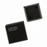
P87C591VFA/00,512 NXP Semiconductors, P87C591VFA/00,512 Datasheet - Page 74

P87C591VFA/00,512
Manufacturer Part Number
P87C591VFA/00,512
Description
IC 80C51 MCU 16K OTP 44-PLCC
Manufacturer
NXP Semiconductors
Series
87Cr
Datasheet
1.P87C591VFA00512.pdf
(160 pages)
Specifications of P87C591VFA/00,512
Core Processor
8051
Core Size
8-Bit
Speed
12MHz
Connectivity
CAN, EBI/EMI, I²C, UART/USART
Peripherals
POR, PWM, WDT
Number Of I /o
32
Program Memory Size
16KB (16K x 8)
Program Memory Type
OTP
Ram Size
512 x 8
Voltage - Supply (vcc/vdd)
4.75 V ~ 5.25 V
Data Converters
A/D 6x10b
Oscillator Type
Internal
Operating Temperature
-40°C ~ 85°C
Package / Case
44-PLCC
Processor Series
P87C5x
Core
80C51
Data Bus Width
8 bit
Data Ram Size
512 B
Interface Type
CAN, I2C, UART
Maximum Clock Frequency
12 MHz
Number Of Programmable I/os
32
Number Of Timers
3
Maximum Operating Temperature
+ 85 C
Mounting Style
SMD/SMT
3rd Party Development Tools
PK51, CA51, A51, ULINK2
Minimum Operating Temperature
- 40 C
On-chip Adc
10 bit, 6 Channel
Lead Free Status / RoHS Status
Lead free / RoHS Compliant
Eeprom Size
-
Lead Free Status / Rohs Status
Details
Other names
568-1256-5
935268182512
P87C591VFAA
935268182512
P87C591VFAA
Available stocks
Company
Part Number
Manufacturer
Quantity
Price
Company:
Part Number:
P87C591VFA/00,512
Manufacturer:
TI
Quantity:
8
Company:
Part Number:
P87C591VFA/00,512
Manufacturer:
NXP Semiconductors
Quantity:
10 000
Philips Semiconductors
The CPU interfaces to the I
special function registers: S1CON (SIO1 control register),
S1STA (SIO1 status register), S1DAT (SIO1 data
register), and S1ADR (SIO1 slave address register). The
SIO1 logic interfaces to the external I
pins: P1.6/SCL (serial clock line) and P1.7/SDA (serial
data line).
A typical I
Figure 31 shows how a data transfer is accomplished on
the bus. Depending on the state of the direction bit (R/W),
two types of data transfers are possible on the I
1. Data transfer from a master transmitter to a slave
2. Data transfer from a slave transmitter to a master
The master device generates all of the serial clock pulses
and the START and STOP conditions. A transfer is ended
with a STOP condition or with a repeated START
condition. Since a repeated START condition is also the
beginning of the next serial transfer, the I
released.
15.1
The on-chip SIO1 logic may operate in the following four
modes:
1. Master Transmitter Mode:
2000 Jul 26
Single-chip 8-bit microcontroller with CAN controller
receiver. The first byte transmitted by the master is the
slave address. Next follows a number of data bytes.
The slave returns an acknowledge bit after each
received byte.
receiver. The first byte (the slave address) is
transmitted by the master. The slave then returns an
acknowledge bit. Next follows the data bytes
transmitted by the slave to the master. The master
returns an acknowledge bit after all received bytes
other than the last byte. At the end of the last received
byte, a not acknowledge is returned.
Serial data output through P1.7/SDA while P1.6/SCL
outputs the serial clock. The first byte transmitted
contains the slave address of the receiving device (7
bits) and the data direction bit. In this case the data
direction bit (R/W) will be logic 0, and we say that a “W”
is transmitted. Thus the first byte transmitted is
SLA+W. Serial data is transmitted 8 bits at a time. After
each byte is transmitted, an acknowledge bit is
received. START and STOP conditions are output to
indicate the beginning and the end of a serial transfer.
Modes of Operation
2
C bus configuration is shown in Figure 30, and
2
C logic via the following four
2
C bus via two port 1
2
C bus will not be
2
C bus:
74
2. Master Receiver Mode:
3. Slave Receiver Mode:
4. Slave Transmitter Mode:
In a given application, SIO1 may operate as a master and
as a slave. In the slave mode, the SIO1 hardware looks for
its own slave address and the general call address. If one
of these addresses is detected, an interrupt is requested.
When the microcontroller wishes to become the bus
master, the hardware waits until the bus is free before the
master mode is entered so that a possible slave action is
not interrupted. If bus arbitration is lost in the master mode,
SIO1 switches to the slave mode immediately and can
detect its own slave address in the same serial transfer.
The first byte transmitted contains the slave address of
the transmitting device (7 bits) and the data direction
bit. In this case the data direction bit (R/W) will be logic
1, and we say that an “R” is transmitted. Thus the first
byte transmitted is SLA+R. Serial data is received via
P1.7/SDA while P1.6/SCL outputs the serial clock.
Serial data is received 8 bits at a time. After each byte
is received, an acknowledge bit is transmitted. START
and STOP conditions are output to indicate the
beginning and end of a serial transfer.
Serial data and the serial clock are received through
P1.7/SDA and P1.6/SCL. After each byte is received,
an acknowledge bit is transmitted. START and STOP
conditions are recognized as the beginning and end of
a serial transfer. Address recognition is performed by
hardware after reception of the slave address and
direction bit.
The first byte is received and handled as in the slave
receiver mode. However, in this mode, the direction bit
will indicate that the transfer direction is reversed.
Serial data is transmitted via P1.7/SDA while the serial
clock is input through P1.6/SCL. START and STOP
conditions are recognized as the beginning and end of
a serial transfer.
Preliminary Specification
P8xC591


