MPC561MZP56 Freescale Semiconductor, MPC561MZP56 Datasheet - Page 44
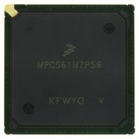
MPC561MZP56
Manufacturer Part Number
MPC561MZP56
Description
IC MPU 32BIT 56MHZ PPC 388-PBGA
Manufacturer
Freescale Semiconductor
Series
MPC5xxr
Datasheet
1.MPC561MZP56.pdf
(1420 pages)
Specifications of MPC561MZP56
Core Processor
PowerPC
Core Size
32-Bit
Speed
56MHz
Connectivity
CAN, EBI/EMI, SCI, SPI, UART/USART
Peripherals
POR, PWM, WDT
Number Of I /o
64
Program Memory Type
ROMless
Ram Size
32K x 8
Voltage - Supply (vcc/vdd)
2.5 V ~ 2.7 V
Data Converters
A/D 32x10b
Oscillator Type
External
Operating Temperature
-40°C ~ 125°C
Package / Case
388-BGA
Controller Family/series
POWER 5xx
No. Of I/o's
56
Ram Memory Size
31KB
Cpu Speed
56MHz
No. Of Timers
32
Embedded Interface Type
QSPI, SCI, UART
No. Of Pwm Channels
12
Rohs Compliant
No
Processor Series
MPC5xx
Core
PowerPC
Data Bus Width
32 bit
Data Ram Size
32 KB
Interface Type
CAN, JTAG, QSPI, SCI, SPI, UART
Maximum Clock Frequency
40 MHz
Number Of Programmable I/os
56
Number Of Timers
22
Operating Supply Voltage
2.6 V to 5 V
Maximum Operating Temperature
+ 85 C
Mounting Style
SMD/SMT
Minimum Operating Temperature
- 40 C
On-chip Adc
2 (10 bit, 32 Channel)
For Use With
MPC564EVB - KIT EVAL FOR MPC561/562/563/564
Lead Free Status / RoHS Status
Contains lead / RoHS non-compliant
Eeprom Size
-
Program Memory Size
-
Lead Free Status / Rohs Status
No
Available stocks
Company
Part Number
Manufacturer
Quantity
Price

Company:
Part Number:
MPC561MZP56
Manufacturer:
Freescale Semiconductor
Quantity:
10 000
Company:
Part Number:
MPC561MZP56R2
Manufacturer:
Freescale Semiconductor
Quantity:
10 000


9-9
9-10
9-11
9-12
9-13
9-14
9-15
9-16
9-17
9-18
9-19
9-20
9-21
9-22
9-23
9-24
9-25
9-26
9-27
9-28
9-29
9-30
9-31
9-32
9-33
9-34
9-35
9-36
9-37
9-38
9-39
9-40
9-41
9-42
10-1
10-2
10-3
10-4
10-5
xliv
Figure
Number
Single Beat Basic Write Cycle Timing – One Wait State ...................................................... 9-14
Single Beat 32-Bit Data Write Cycle Timing — 16-Bit Port Size ......................................... 9-15
Read Followed by Write when Pre-Discharge Mode is Enabled, and EHTR is Set .............. 9-17
Basic Flow Diagram Of A Burst-Read Cycle......................................................................... 9-21
Burst-Read Cycle – 32-Bit Port Size – Zero Wait State......................................................... 9-21
Burst-Read Cycle – 32-Bit Port Size – One Wait State.......................................................... 9-22
Burst-Read Cycle – 32-Bit Port Size – Wait States Between Beats ....................................... 9-23
Burst-Read Cycle – 16-Bit Port Size ...................................................................................... 9-24
Basic Flow Diagram of a Burst-Write Cycle.......................................................................... 9-26
Burst-Write Cycle, 32-Bit Port Size, Zero Wait States
(Only for External Master Memory Controller Service Support)........................................... 9-26
Burst-Inhibit Read Cycle, 32-Bit Port Size (Emulated Burst)................................................ 9-27
Non-Wrap Burst with Three Beats ......................................................................................... 9-28
Non-Wrap Burst with One Data Beat ..................................................................................... 9-29
Internal Operand Representation ............................................................................................ 9-30
Interface To Different Port Size Devices................................................................................ 9-31
Bus Arbitration Flowchart ...................................................................................................... 9-33
Master Signals Basic Connection ........................................................................................... 9-34
Bus Arbitration Timing Diagram............................................................................................ 9-35
Internal Bus Arbitration State Machine .................................................................................. 9-36
Termination Signals Protocol Basic Connection .................................................................... 9-41
Termination Signals Protocol Timing Diagram...................................................................... 9-41
Reservation on Local Bus ....................................................................................................... 9-43
Reservation on Multi-level Bus Hierarchy ............................................................................. 9-44
Retry Transfer Timing – Internal Arbiter ............................................................................... 9-46
Retry Transfer Timing – External Arbiter .............................................................................. 9-47
Retry on Burst Cycle............................................................................................................... 9-48
Basic Flow of an External Master Read Access ..................................................................... 9-50
Basic Flow of an External Master Write Access .................................................................... 9-51
Peripheral Mode: External Master Reads from MPC561/MPC563 (Two Wait States) ......... 9-52
Peripheral Mode: External Master Writes to MPC561/MPC563 (Two Wait States)............ 9-53
Flow of Retry of External Master Read Access ..................................................................... 9-54
Retry of External Master Access (Internal Arbiter)................................................................ 9-55
Instruction Show Cycle Transaction....................................................................................... 9-57
Data Show Cycle Transaction................................................................................................. 9-58
Memory Controller Function within the USIU....................................................................... 10-1
Memory Controller Block Diagram........................................................................................ 10-2
MPC561/MPC563 Simple System Configuration .................................................................. 10-3
Bank Base Address and Match Structure ............................................................................... 10-4
A 4-2-2-2 Burst Read Cycle (One Wait State Between Bursts) ............................................. 10-9
MPC561/MPC563 Reference Manual, Rev. 1.2
Figures
Title
Freescale Semiconductor
Number
Page
Related parts for MPC561MZP56
Image
Part Number
Description
Manufacturer
Datasheet
Request
R

Part Number:
Description:
MPC5 1K0 5%
Manufacturer:
TE Connectivity
Datasheet:


Part Number:
Description:
MPC5 500R 5%
Manufacturer:
TE Connectivity
Datasheet:

Part Number:
Description:
MPC5 5K0 5%
Manufacturer:
Tyco Electronics
Datasheet:
Part Number:
Description:
MPC5 5R0 5%
Manufacturer:
Tyco Electronics
Datasheet:
Part Number:
Description:
MPC5 50K 5%
Manufacturer:
Tyco Electronics
Datasheet:
Part Number:
Description:
MPC5 1R0 5%
Manufacturer:
Tyco Electronics
Datasheet:

Part Number:
Description:
Manufacturer:
Freescale Semiconductor, Inc
Datasheet:
Part Number:
Description:
Manufacturer:
Freescale Semiconductor, Inc
Datasheet:
Part Number:
Description:
Manufacturer:
Freescale Semiconductor, Inc
Datasheet:
Part Number:
Description:
Manufacturer:
Freescale Semiconductor, Inc
Datasheet:
Part Number:
Description:
Manufacturer:
Freescale Semiconductor, Inc
Datasheet: