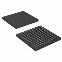
AT91SAM9R64-CU-999 Atmel, AT91SAM9R64-CU-999 Datasheet - Page 210

AT91SAM9R64-CU-999
Manufacturer Part Number
AT91SAM9R64-CU-999
Description
IC MCU ARM9 64K SRAM 144LFBGA
Manufacturer
Atmel
Series
AT91SAMr
Datasheet
1.AT91SAM9R64-CU.pdf
(903 pages)
Specifications of AT91SAM9R64-CU-999
Core Processor
ARM9
Core Size
16/32-Bit
Speed
240MHz
Connectivity
EBI/EMI, I²C, MMC, SPI, SSC, UART/USART, USB
Peripherals
AC'97, POR, PWM, WDT
Number Of I /o
49
Program Memory Size
32KB (32K x 8)
Program Memory Type
ROM
Ram Size
72K x 8
Voltage - Supply (vcc/vdd)
1.08 V ~ 1.32 V
Data Converters
A/D 3x10b
Oscillator Type
Internal
Operating Temperature
-40°C ~ 85°C
Package / Case
144-LFBGA
Processor Series
AT91SAMx
Core
ARM926EJ-S
Data Bus Width
32 bit
Data Ram Size
64 KB
Interface Type
SPI, TWI, UART
Maximum Clock Frequency
240 MHz
Number Of Programmable I/os
118
Operating Supply Voltage
1.65 V to 3.6 V
Maximum Operating Temperature
+ 85 C
Mounting Style
SMD/SMT
3rd Party Development Tools
JTRACE-ARM-2M, MDK-ARM, RL-ARM, ULINK2
Development Tools By Supplier
AT91SAM-ICE, AT91-ISP, AT91SAM9RL-EK
Minimum Operating Temperature
- 40 C
For Use With
AT91SAM-ICE - EMULATOR FOR AT91 ARM7/ARM9
Lead Free Status / RoHS Status
Lead free / RoHS Compliant
Eeprom Size
-
Lead Free Status / Rohs Status
Details
Available stocks
Company
Part Number
Manufacturer
Quantity
Price
- Current page: 210 of 903
- Download datasheet (13Mb)
23.5
23.5.1
Figure 23-2. Write Burst, 32-bit SDRAM Access
210
SDRAMC_A[12:0]
Functional Description
D[31:0]
SDWE
SDCS
SDCK
AT91SAM9R64/RL64 Preliminary
RAS
CAS
SDRAM Controller Write Cycle
The SDRAM Controller allows burst access or single access. In both cases, the SDRAM control-
ler keeps track of the active row in each bank, thus maximizing performance. To initiate a burst
access, the SDRAM Controller uses the transfer type signal provided by the master requesting
the access. If the next access is a sequential write access, writing to the SDRAM device is car-
ried out. If the next access is a write-sequential access, but the current access is to a boundary
page, or if the next access is in another row, then the SDRAM Controller generates a precharge
command, activates the new row and initiates a write command. To comply with SDRAM timing
parameters, additional clock cycles are inserted between precharge/active (t
active/write (t
Configuration Register” on page
Row n
t
RCD
= 3
col a
RCD
Dna
) commands. For definition of these timing parameters, refer to the
col b
Dnb
col c
Dnc
221. This is described in
col d
Dnd
col e
Dne
col f
Dnf
col g
Dng
Figure 23-2
col h
Dnh
col i
Dni
below.
col j
Dnj
6289C–ATARM–28-May-09
RP
) commands and
col k
Dnk
“SDRAMC
col l
Dnl
Related parts for AT91SAM9R64-CU-999
Image
Part Number
Description
Manufacturer
Datasheet
Request
R

Part Number:
Description:
MCU ARM9 64K SRAM 144-LFBGA
Manufacturer:
Atmel
Datasheet:

Part Number:
Description:
MCU, MPU & DSP Development Tools KICKSTART KIT FOR AT91SAM9 PLUS
Manufacturer:
IAR Systems

Part Number:
Description:
DEV KIT FOR AVR/AVR32
Manufacturer:
Atmel
Datasheet:

Part Number:
Description:
INTERVAL AND WIPE/WASH WIPER CONTROL IC WITH DELAY
Manufacturer:
ATMEL Corporation
Datasheet:

Part Number:
Description:
Low-Voltage Voice-Switched IC for Hands-Free Operation
Manufacturer:
ATMEL Corporation
Datasheet:

Part Number:
Description:
MONOLITHIC INTEGRATED FEATUREPHONE CIRCUIT
Manufacturer:
ATMEL Corporation
Datasheet:

Part Number:
Description:
AM-FM Receiver IC U4255BM-M
Manufacturer:
ATMEL Corporation
Datasheet:

Part Number:
Description:
Monolithic Integrated Feature Phone Circuit
Manufacturer:
ATMEL Corporation
Datasheet:

Part Number:
Description:
Multistandard Video-IF and Quasi Parallel Sound Processing
Manufacturer:
ATMEL Corporation
Datasheet:

Part Number:
Description:
High-performance EE PLD
Manufacturer:
ATMEL Corporation
Datasheet:

Part Number:
Description:
8-bit Flash Microcontroller
Manufacturer:
ATMEL Corporation
Datasheet:


