AT91SAM9R64-CU-999 Atmel, AT91SAM9R64-CU-999 Datasheet - Page 3
AT91SAM9R64-CU-999
Manufacturer Part Number
AT91SAM9R64-CU-999
Description
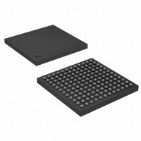
IC MCU ARM9 64K SRAM 144LFBGA
Manufacturer
Atmel
Series
AT91SAMr
Datasheet
1.AT91SAM9R64-CU.pdf
(903 pages)
Specifications of AT91SAM9R64-CU-999
Core Processor
ARM9
Core Size
16/32-Bit
Speed
240MHz
Connectivity
EBI/EMI, I²C, MMC, SPI, SSC, UART/USART, USB
Peripherals
AC'97, POR, PWM, WDT
Number Of I /o
49
Program Memory Size
32KB (32K x 8)
Program Memory Type
ROM
Ram Size
72K x 8
Voltage - Supply (vcc/vdd)
1.08 V ~ 1.32 V
Data Converters
A/D 3x10b
Oscillator Type
Internal
Operating Temperature
-40°C ~ 85°C
Package / Case
144-LFBGA
Processor Series
AT91SAMx
Core
ARM926EJ-S
Data Bus Width
32 bit
Data Ram Size
64 KB
Interface Type
SPI, TWI, UART
Maximum Clock Frequency
240 MHz
Number Of Programmable I/os
118
Operating Supply Voltage
1.65 V to 3.6 V
Maximum Operating Temperature
+ 85 C
Mounting Style
SMD/SMT
3rd Party Development Tools
JTRACE-ARM-2M, MDK-ARM, RL-ARM, ULINK2
Development Tools By Supplier
AT91SAM-ICE, AT91-ISP, AT91SAM9RL-EK
Minimum Operating Temperature
- 40 C
For Use With
AT91SAM-ICE - EMULATOR FOR AT91 ARM7/ARM9
Lead Free Status / RoHS Status
Lead free / RoHS Compliant
Eeprom Size
-
Lead Free Status / Rohs Status
Details
Available stocks
Company
Part Number
Manufacturer
Quantity
Price


•
•
•
•
1. Description
6289C–ATARM–28-May-09
SAM-BA
IEEE
Required Power Supplies:
Available in a 144-ball BGA (AT91SAM9R64) and a 217-ball LFBGA (AT91SAM9RL64) Package
– Master, Multi-master and Slave Mode Operation
– Bit Rate: Up to 400 Kbits
– General Call Supported in Slave Mode
– Connection to Peripheral DMA Controller (PDC) Channel Capabilities Optimizes Data Transfers in Master Mode Only
– Default Boot Program
– Interface with SAM-BA Graphic User Interface
– 1.08 to 1.32V for VDDCORE, VDDUTMIC, VDDPLLB and VDDBU
– 3.0V to 3.6V for VDDPLLA, VDDANA, VDDUTMII and VDDIOP
– Programmable 1.65V to 1.95V or 3.0V to 3.6V for VDDIOM
(TWI0 only)
®
1149.1 JTAG Boundary Scan on All Digital Pins
®
Boot Assistant
The AT91SAM9R64/RL64 device is based on the integration of an ARM926EJ-S processor with
a large fast SRAM and a wide range of peripherals.
The AT91SAM9R64/RL64 embeds one USB Device High Speed Controller, one LCD Controller
(for AT91SAM9RL64 only), one AC97 controller, a 2-channel DMA Controller, four USARTs, two
SSCs, one SPI, two TWIs, three Timer Counter channels, a 4-channel PWM generator, one Mul-
timedia Card interface and a 6-channel Analog-to-digital converter that also provides resistive
touch screen management.
The AT91SAM9R64/RL64 is architectured on a 6-layer bus matrix. It also features an External
Bus Interface capable of interfacing with a wide range of memory and peripheral devices.
Some features are not available for AT91SAM9R64 in the 144-ball BGA package.
Separate block diagrams and PIO multiplexing are provided in this document.
features and signals of AT91SAM9RL64 that are not available or partially available for
AT91SAM9R64. When the signal is multiplexed on a PIO, the PIO line is specified.
Table 1-1.
Feature
AC97
EBI
LCDC
Unavailable or Partially Available Features and Signals in AT91SAM9R64
Full/Partial
Full
Partial
Full
Signal
AC97FS
AC97CK
AC97TX
AC97RX
D16-D31
NCS2
NCS5/CFCS1
LCDMOD
LCDCC
LCDVSYNC
LCDHSYNC
LCDDOTCK
LCDDEN
LCDD0-LCDD23
AT91SAM9R64/RL64 Preliminary
Peripheral A
PD1
PD2
PD3
PD4
PB16-PB31
PD0
PD13
PC2
PC3
PC4
PC5
PC6
PC7
PC8-PC31
Peripheral B
-
-
-
Table 1-1
lists the
3
Related parts for AT91SAM9R64-CU-999
Image
Part Number
Description
Manufacturer
Datasheet
Request
R

Part Number:
Description:
MCU ARM9 64K SRAM 144-LFBGA
Manufacturer:
Atmel
Datasheet:

Part Number:
Description:
MCU, MPU & DSP Development Tools KICKSTART KIT FOR AT91SAM9 PLUS
Manufacturer:
IAR Systems

Part Number:
Description:
DEV KIT FOR AVR/AVR32
Manufacturer:
Atmel
Datasheet:

Part Number:
Description:
INTERVAL AND WIPE/WASH WIPER CONTROL IC WITH DELAY
Manufacturer:
ATMEL Corporation
Datasheet:
Part Number:
Description:
Low-Voltage Voice-Switched IC for Hands-Free Operation
Manufacturer:
ATMEL Corporation
Datasheet:
Part Number:
Description:
MONOLITHIC INTEGRATED FEATUREPHONE CIRCUIT
Manufacturer:
ATMEL Corporation
Datasheet:
Part Number:
Description:
AM-FM Receiver IC U4255BM-M
Manufacturer:
ATMEL Corporation
Datasheet:
Part Number:
Description:
Monolithic Integrated Feature Phone Circuit
Manufacturer:
ATMEL Corporation
Datasheet:
Part Number:
Description:
Multistandard Video-IF and Quasi Parallel Sound Processing
Manufacturer:
ATMEL Corporation
Datasheet:
Part Number:
Description:
High-performance EE PLD
Manufacturer:
ATMEL Corporation
Datasheet:
Part Number:
Description:
8-bit Flash Microcontroller
Manufacturer:
ATMEL Corporation
Datasheet: