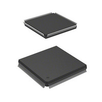
HD6417750RF200DV Renesas Electronics America, HD6417750RF200DV Datasheet - Page 148

HD6417750RF200DV
Manufacturer Part Number
HD6417750RF200DV
Description
MPU 1.5/3.3V 0K I-TEMP PB-FREE 2
Manufacturer
Renesas Electronics America
Series
SuperH® SH7750r
Datasheet
1.D6417750RBP240DV.pdf
(1164 pages)
Specifications of HD6417750RF200DV
Core Processor
SH-4
Core Size
32-Bit
Speed
200MHz
Connectivity
EBI/EMI, FIFO, SCI, SmartCard
Peripherals
DMA, POR, WDT
Number Of I /o
28
Program Memory Type
ROMless
Ram Size
48K x 8
Voltage - Supply (vcc/vdd)
1.35 V ~ 1.6 V
Oscillator Type
External
Operating Temperature
-40°C ~ 85°C
Package / Case
208-QFP Exposed Pad, 208-eQFP, 208-HQFP
Lead Free Status / RoHS Status
Lead free / RoHS Compliant
Eeprom Size
-
Program Memory Size
-
Data Converters
-
Available stocks
Company
Part Number
Manufacturer
Quantity
Price
Company:
Part Number:
HD6417750RF200DV
Manufacturer:
FREESCALE
Quantity:
450
- Current page: 148 of 1164
- Download datasheet (7Mb)
Section 2 Programming Model
2.2.4
Status register, SR (32 bits, privilege protection, initial value = 0111 0000 0000 0000 0000
00XX 1111 00XX (X: undefined))
Note: —: Reserved. These bits are always read as 0, and should only be written with 0.
• MD: Processor mode
• RB: General register bank specifier in privileged mode (set to 1 by a reset, exception, or
• BL: Exception/interrupt block bit (set to 1 by a reset, exception, or interrupt)
• FD: FPU disable bit (cleared to 0 by a reset)
• M, Q: Used by the DIV0S, DIV0U, and DIV1 instructions.
• IMASK: Interrupt mask level
• S: Specifies a saturation operation for a MAC instruction.
• T: True/false condition or carry/borrow bit
Rev.7.00 Oct. 10, 2008 Page 62 of 1074
REJ09B0366-0700
— MD RB BL
31 30 29 28 27
MD = 0: User mode (some instructions cannot be executed, and some resources cannot be
accessed)
MD = 1: Privileged mode
interrupt)
RB = 0: R0_BANK0–R7_BANK0 are accessed as general registers R0–R7. (R0_BANK1–
R7_BANK1 can be accessed using LDC/STC R0_BANK–R7_BANK instructions.)
RB = 1: R0_BANK1–R7_BANK1 are accessed as general registers R0–R7. (R0_BANK0–
R7_BANK0 can be accessed using LDC/STC R0_BANK–R7_BANK instructions.)
BL = 1: Interrupt requests are masked. If a general exception other than a user break occurs
while BL = 1, the processor switches to the reset state.
FD = 1: An FPU instruction causes a general FPU disable exception, and if the FPU instruction
is in a delay slot, a slot FPU disable exception is generated. (FPU instructions: H'F***
instructions, LDC(.L)/STS(.L) instructions for FPUL/FPSCR)
External interrupts of a same level or a lower level than IMASK are masked.
Control Registers
—
16 15 14
FD
—
10
M
9
Q
8
7
IMASK
4
3
—
2
S
1
T
0
Related parts for HD6417750RF200DV
Image
Part Number
Description
Manufacturer
Datasheet
Request
R

Part Number:
Description:
KIT STARTER FOR M16C/29
Manufacturer:
Renesas Electronics America
Datasheet:

Part Number:
Description:
KIT STARTER FOR R8C/2D
Manufacturer:
Renesas Electronics America
Datasheet:

Part Number:
Description:
R0K33062P STARTER KIT
Manufacturer:
Renesas Electronics America
Datasheet:

Part Number:
Description:
KIT STARTER FOR R8C/23 E8A
Manufacturer:
Renesas Electronics America
Datasheet:

Part Number:
Description:
KIT STARTER FOR R8C/25
Manufacturer:
Renesas Electronics America
Datasheet:

Part Number:
Description:
KIT STARTER H8S2456 SHARPE DSPLY
Manufacturer:
Renesas Electronics America
Datasheet:

Part Number:
Description:
KIT STARTER FOR R8C38C
Manufacturer:
Renesas Electronics America
Datasheet:

Part Number:
Description:
KIT STARTER FOR R8C35C
Manufacturer:
Renesas Electronics America
Datasheet:

Part Number:
Description:
KIT STARTER FOR R8CL3AC+LCD APPS
Manufacturer:
Renesas Electronics America
Datasheet:

Part Number:
Description:
KIT STARTER FOR RX610
Manufacturer:
Renesas Electronics America
Datasheet:

Part Number:
Description:
KIT STARTER FOR R32C/118
Manufacturer:
Renesas Electronics America
Datasheet:

Part Number:
Description:
KIT DEV RSK-R8C/26-29
Manufacturer:
Renesas Electronics America
Datasheet:

Part Number:
Description:
KIT STARTER FOR SH7124
Manufacturer:
Renesas Electronics America
Datasheet:

Part Number:
Description:
KIT STARTER FOR H8SX/1622
Manufacturer:
Renesas Electronics America
Datasheet:

Part Number:
Description:
KIT DEV FOR SH7203
Manufacturer:
Renesas Electronics America
Datasheet:


