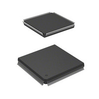
HD6417750RF200DV Renesas Electronics America, HD6417750RF200DV Datasheet - Page 69

HD6417750RF200DV
Manufacturer Part Number
HD6417750RF200DV
Description
MPU 1.5/3.3V 0K I-TEMP PB-FREE 2
Manufacturer
Renesas Electronics America
Series
SuperH® SH7750r
Datasheet
1.D6417750RBP240DV.pdf
(1164 pages)
Specifications of HD6417750RF200DV
Core Processor
SH-4
Core Size
32-Bit
Speed
200MHz
Connectivity
EBI/EMI, FIFO, SCI, SmartCard
Peripherals
DMA, POR, WDT
Number Of I /o
28
Program Memory Type
ROMless
Ram Size
48K x 8
Voltage - Supply (vcc/vdd)
1.35 V ~ 1.6 V
Oscillator Type
External
Operating Temperature
-40°C ~ 85°C
Package / Case
208-QFP Exposed Pad, 208-eQFP, 208-HQFP
Lead Free Status / RoHS Status
Lead free / RoHS Compliant
Eeprom Size
-
Program Memory Size
-
Data Converters
-
Available stocks
Company
Part Number
Manufacturer
Quantity
Price
Company:
Part Number:
HD6417750RF200DV
Manufacturer:
FREESCALE
Quantity:
450
- Current page: 69 of 1164
- Download datasheet (7Mb)
Figure 13.38 Burst Read Cycle for Different Bank and Row Address Following Preceding
Figure 13.39 Auto-Refresh Operation ......................................................................................... 485
Figure 13.40 Synchronous DRAM Auto-Refresh Timing........................................................... 486
Figure 13.41 Synchronous DRAM Self-Refresh Timing ............................................................ 487
Figure 13.42 (1) Synchronous DRAM Mode Write Timing (PALL) ........................................ 490
Figure 13.42 (2) Synchronous DRAM Mode Write Timing (Mode Register Set)..................... 491
Figure 13.43 Basic Timing of Synchronous DRAM Burst Read (Burst Length = 4).................. 492
Figure 13.44 Basic Timing of a Burst Write to Synchronous DRAM......................................... 494
Figure 13.45 Example of the Connection of Synchronous DRAM with 64-bit Bus Width
Figure 13.46 Synchronous DRAM Auto-Refresh Timing with 64-Bit Bus Width
Figure 13.47 Burst ROM Basic Access Timing .......................................................................... 498
Figure 13.48 Burst ROM Wait Access Timing ........................................................................... 499
Figure 13.49 Burst ROM Wait Access Timing ........................................................................... 500
Figure 13.50 Example of PCMCIA Interface .............................................................................. 504
Figure 13.51 Basic Timing for PCMCIA Memory Card Interface .............................................. 505
Figure 13.52 Wait Timing for PCMCIA Memory Card Interface ............................................... 506
Figure 13.53 PCMCIA Space Allocation .................................................................................... 507
Figure 13.54 Basic Timing for PCMCIA I/O Card Interface ...................................................... 508
Figure 13.55 Wait Timing for PCMCIA I/O Card Interface ....................................................... 509
Figure 13.56 Dynamic Bus Sizing Timing for PCMCIA I/O Card Interface .............................. 510
Figure 13.57 Example of 64-Bit Data Width MPX Connection.................................................. 512
Figure 13.58 MPX Interface Timing 1 (Single Read Cycle, AnW = 0, No External Wait,
Figure 13.59 MPX Interface Timing 2 (Single Read, AnW = 0, One External Wait Inserted,
Figure 13.60 MPX Interface Timing 3 (Single Write Cycle, AnW = 0, No Wait,
Figure 13.61 MPX Interface Timing 4 (Single Write, AnW = 1, One External Wait Inserted,
Figure 13.62 MPX Interface Timing 5 (Burst Read Cycle, AnW = 0, No External Wait,
Figure 13.63 MPX Interface Timing 6 (Burst Read Cycle, AnW = 0, External Wait Control,
Figure 13.64 MPX Interface Timing 7 (Burst Write Cycle, AnW = 0, No External Wait,
Figure 13.65 MPX Interface Timing 8 (Burst Write Cycle, AnW = 1, External Wait Control,
Burst Read Cycle.................................................................................................... 483
(256 Mbits)............................................................................................................. 495
(TRAS[2:0] = 001, TRC[2:0] = 001)...................................................................... 496
Bus Width: 64 Bits)................................................................................................ 513
Bus Width: 64 Bits)................................................................................................ 514
Bus Width: 64 Bits)................................................................................................ 515
Bus Width: 64 Bits)................................................................................................ 516
Bus Width: 64 Bits, Transfer Data Size: 32 Bytes) ............................................... 517
Bus Width: 64 Bits, Transfer Data Size: 32 Bytes) ............................................... 518
Bus Width: 64 Bits, Transfer Data Size: 32 Bytes) ............................................... 519
Bus Width: 64 Bits, Transfer Data Size: 32 Bytes) ............................................... 520
Rev.7.00 Oct. 10, 2008 Page lxvii of lxxxiv
REJ09B0366-0700
Related parts for HD6417750RF200DV
Image
Part Number
Description
Manufacturer
Datasheet
Request
R

Part Number:
Description:
KIT STARTER FOR M16C/29
Manufacturer:
Renesas Electronics America
Datasheet:

Part Number:
Description:
KIT STARTER FOR R8C/2D
Manufacturer:
Renesas Electronics America
Datasheet:

Part Number:
Description:
R0K33062P STARTER KIT
Manufacturer:
Renesas Electronics America
Datasheet:

Part Number:
Description:
KIT STARTER FOR R8C/23 E8A
Manufacturer:
Renesas Electronics America
Datasheet:

Part Number:
Description:
KIT STARTER FOR R8C/25
Manufacturer:
Renesas Electronics America
Datasheet:

Part Number:
Description:
KIT STARTER H8S2456 SHARPE DSPLY
Manufacturer:
Renesas Electronics America
Datasheet:

Part Number:
Description:
KIT STARTER FOR R8C38C
Manufacturer:
Renesas Electronics America
Datasheet:

Part Number:
Description:
KIT STARTER FOR R8C35C
Manufacturer:
Renesas Electronics America
Datasheet:

Part Number:
Description:
KIT STARTER FOR R8CL3AC+LCD APPS
Manufacturer:
Renesas Electronics America
Datasheet:

Part Number:
Description:
KIT STARTER FOR RX610
Manufacturer:
Renesas Electronics America
Datasheet:

Part Number:
Description:
KIT STARTER FOR R32C/118
Manufacturer:
Renesas Electronics America
Datasheet:

Part Number:
Description:
KIT DEV RSK-R8C/26-29
Manufacturer:
Renesas Electronics America
Datasheet:

Part Number:
Description:
KIT STARTER FOR SH7124
Manufacturer:
Renesas Electronics America
Datasheet:

Part Number:
Description:
KIT STARTER FOR H8SX/1622
Manufacturer:
Renesas Electronics America
Datasheet:

Part Number:
Description:
KIT DEV FOR SH7203
Manufacturer:
Renesas Electronics America
Datasheet:


