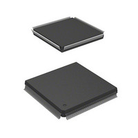
HD6417750RF200DV Renesas Electronics America, HD6417750RF200DV Datasheet - Page 77

HD6417750RF200DV
Manufacturer Part Number
HD6417750RF200DV
Description
MPU 1.5/3.3V 0K I-TEMP PB-FREE 2
Manufacturer
Renesas Electronics America
Series
SuperH® SH7750r
Datasheet
1.D6417750RBP240DV.pdf
(1164 pages)
Specifications of HD6417750RF200DV
Core Processor
SH-4
Core Size
32-Bit
Speed
200MHz
Connectivity
EBI/EMI, FIFO, SCI, SmartCard
Peripherals
DMA, POR, WDT
Number Of I /o
28
Program Memory Type
ROMless
Ram Size
48K x 8
Voltage - Supply (vcc/vdd)
1.35 V ~ 1.6 V
Oscillator Type
External
Operating Temperature
-40°C ~ 85°C
Package / Case
208-QFP Exposed Pad, 208-eQFP, 208-HQFP
Lead Free Status / RoHS Status
Lead free / RoHS Compliant
Eeprom Size
-
Program Memory Size
-
Data Converters
-
Available stocks
Company
Part Number
Manufacturer
Quantity
Price
Company:
Part Number:
HD6417750RF200DV
Manufacturer:
FREESCALE
Quantity:
450
- Current page: 77 of 1164
- Download datasheet (7Mb)
Figure 22.38 DRAM Bus Cycle (EDO Mode, RCD[1:0] = 00, AnW[2:0] = 000,
Figure 22.39 DRAM Burst Bus Cycle (EDO Mode, RCD[1:0] = 00, AnW[2:0] = 000,
Figure 22.40 DRAM Burst Bus Cycle (EDO Mode, RCD[1:0] = 01, AnW[2:0] = 001,
Figure 22.41 DRAM Burst Bus Cycle (EDO Mode, RCD[1:0] = 01, AnW[2:0] = 001,
Figure 22.42 DRAM Burst Bus Cycle: RAS Down Mode State (EDO Mode, RCD[1:0] = 00,
Figure 22.43 DRAM Burst Bus Cycle: RAS Down Mode Continuation (EDO Mode,
Figure 22.44 DRAM Burst Bus Cycle (Fast Page Mode, RCD[1:0] = 00, AnW[2:0] = 000,
Figure 22.45 DRAM Burst Bus Cycle (Fast Page Mode, RCD[1:0] = 01, AnW[2:0] = 001,
Figure 22.46 DRAM Burst Bus Cycle (Fast Page Mode, RCD[1:0] = 01, AnW[2:0] = 001,
Figure 22.47 DRAM Burst Bus Cycle: RAS Down Mode State (Fast Page Mode,
Figure 22.48 DRAM Burst Bus Cycle: RAS Down Mode Continuation (Fast Page Mode,
Figure 22.49 DRAM Bus Cycle: DRAM CAS-Before-RAS Refresh (TRAS[2:0] = 000,
Figure 22.50 DRAM Bus Cycle: DRAM CAS-Before-RAS Refresh (TRAS[2:0] = 001,
Figure 22.51 DRAM Bus Cycle: DRAM Self-Refresh (TRC[2:0] = 001) .................................. 993
Figure 22.52 PCMCIA Memory Bus Cycle (1) TED[2:0] = 000, TEH[2:0] = 000, No Wait
Figure 22.53 PCMCIA I/O Bus Cycle (1) TED[2:0] = 000, TEH[2:0] = 000, No Wait
Figure 22.54 PCMCIA I/O Bus Cycle (TED[2:0] = 001, TEH[2:0] = 001, One Internal Wait,
Figure 22.55 MPX Basic Bus Cycle: Read (1) 1st Data (One Internal Wait) (2) 1st Data
Figure 22.56 MPX Basic Bus Cycle: Write (1) 1st Data (No Wait) (2) 1st Data (One Internal
Figure 22.57 MPX Bus Cycle: Burst Read (1) 1st Data (One Internal Wait), 2nd to 8th Data
TPC[2:0] = 001) ..................................................................................................... 980
TPC[2:0] = 001) ..................................................................................................... 981
TPC[2:0] = 001) ..................................................................................................... 982
TPC[2:0] = 001, 2-Cycle CAS Negate Pulse Width) ............................................. 983
AnW[2:0] = 000).................................................................................................... 984
RCD[1:0] = 00, AnW[2:0] = 000).......................................................................... 985
TPC[2:0] = 001) ..................................................................................................... 986
TPC[2:0] = 001) ..................................................................................................... 987
TPC[2:0] = 001, 2-Cycle CAS Negate Pulse Width) ............................................. 988
RCD[1:0] = 00, AnW[2:0] = 000).......................................................................... 989
RCD[1:0] = 00, AnW[2:0] = 000).......................................................................... 990
TRC[2:0] = 001)..................................................................................................... 991
TRC[2:0] = 001)..................................................................................................... 992
(2) TED[2:0] = 001, TEH[2:0] = 001, One Internal Wait + One External Wait .... 994
(2) TED[2:0] = 001, TEH[2:0] = 001, One Internal Wait + One External Wait .... 995
Bus Sizing) ............................................................................................................. 996
(One Internal Wait + One External Wait) .............................................................. 997
Wait) (3) 1st Data (One Internal Wait + One External Wait)................................. 998
(One Internal Wait) (2) 1st Data (One Internal Wait), 2nd to 4th Data
(One Internal Wait + One External Wait) .............................................................. 999
Rev.7.00 Oct. 10, 2008 Page lxxv of lxxxiv
REJ09B0366-0700
Related parts for HD6417750RF200DV
Image
Part Number
Description
Manufacturer
Datasheet
Request
R

Part Number:
Description:
KIT STARTER FOR M16C/29
Manufacturer:
Renesas Electronics America
Datasheet:

Part Number:
Description:
KIT STARTER FOR R8C/2D
Manufacturer:
Renesas Electronics America
Datasheet:

Part Number:
Description:
R0K33062P STARTER KIT
Manufacturer:
Renesas Electronics America
Datasheet:

Part Number:
Description:
KIT STARTER FOR R8C/23 E8A
Manufacturer:
Renesas Electronics America
Datasheet:

Part Number:
Description:
KIT STARTER FOR R8C/25
Manufacturer:
Renesas Electronics America
Datasheet:

Part Number:
Description:
KIT STARTER H8S2456 SHARPE DSPLY
Manufacturer:
Renesas Electronics America
Datasheet:

Part Number:
Description:
KIT STARTER FOR R8C38C
Manufacturer:
Renesas Electronics America
Datasheet:

Part Number:
Description:
KIT STARTER FOR R8C35C
Manufacturer:
Renesas Electronics America
Datasheet:

Part Number:
Description:
KIT STARTER FOR R8CL3AC+LCD APPS
Manufacturer:
Renesas Electronics America
Datasheet:

Part Number:
Description:
KIT STARTER FOR RX610
Manufacturer:
Renesas Electronics America
Datasheet:

Part Number:
Description:
KIT STARTER FOR R32C/118
Manufacturer:
Renesas Electronics America
Datasheet:

Part Number:
Description:
KIT DEV RSK-R8C/26-29
Manufacturer:
Renesas Electronics America
Datasheet:

Part Number:
Description:
KIT STARTER FOR SH7124
Manufacturer:
Renesas Electronics America
Datasheet:

Part Number:
Description:
KIT STARTER FOR H8SX/1622
Manufacturer:
Renesas Electronics America
Datasheet:

Part Number:
Description:
KIT DEV FOR SH7203
Manufacturer:
Renesas Electronics America
Datasheet:


