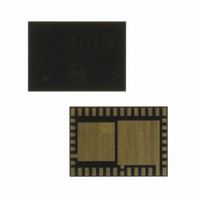
SI1005-C-GM Silicon Laboratories Inc, SI1005-C-GM Datasheet - Page 146

SI1005-C-GM
Manufacturer Part Number
SI1005-C-GM
Description
IC TXRX MCU + EZRADIOPRO
Manufacturer
Silicon Laboratories Inc
Specifications of SI1005-C-GM
Package / Case
42-QFN
Frequency
240MHz ~ 960MHz
Data Rate - Maximum
256kbps
Modulation Or Protocol
FSK, GFSK, OOK
Applications
General Purpose
Power - Output
13dBm
Sensitivity
-121dBm
Voltage - Supply
0.9 V ~ 1.8 V
Current - Receiving
18.5mA
Current - Transmitting
30mA
Data Interface
PCB, Surface Mount
Memory Size
32kB Flash, 4kB RAM
Antenna Connector
PCB, Surface Mount
Number Of Receivers
1
Number Of Transmitters
1
Wireless Frequency
240 MHz to 960 MHz
Interface Type
UART, SMBus, SPI, PCA
Output Power
13 dBm
Operating Supply Voltage
0.9 V to 3.6 V
Maximum Operating Temperature
+ 85 C
Mounting Style
SMD/SMT
Maximum Supply Current
4.1 mA
Minimum Operating Temperature
- 40 C
Modulation
FSK, GFSK, OOK
Protocol Supported
C2, SMBus
Core
8051
Program Memory Type
Flash
Program Memory Size
32 KB
Data Ram Size
4352 B
Supply Current (max)
4.1 mA
Lead Free Status / RoHS Status
Lead free / RoHS Compliant
Operating Temperature
-
Lead Free Status / Rohs Status
Lead free / RoHS Compliant
Other names
336-1875-5
Available stocks
Company
Part Number
Manufacturer
Quantity
Price
Company:
Part Number:
SI1005-C-GM
Manufacturer:
Silicon Labs
Quantity:
135
- Current page: 146 of 376
- Download datasheet (3Mb)
Si1000/1/2/3/4/5
5. Make certain that all writes to the RSTSRC (Reset Sources) register use direct assignment operators
6. Make certain that all writes to the RSTSRC register explicitly set the PORSF bit to a 1. Areas to check
13.5.2. PSWE Maintenance
7. Reduce the number of places in code where the PSWE bit (b0 in PSCTL) is set to a 1. There should be
8. Minimize the number of variable accesses while PSWE is set to a 1. Handle pointer address updates
9. Disable interrupts prior to setting PSWE to a 1 and leave them disabled until after PSWE has been
10.Make certain that the Flash write and erase pointer variables are not located in XRAM. See your
11. Add address bounds checking to the routines that write or erase Flash memory to ensure that a routine
13.5.3. System Clock
12.If operating from an external crystal, be advised that crystal performance is susceptible to electrical
13.If operating from the external oscillator, switch to the internal oscillator during Flash write or erase
Additional Flash recommendations and example code can be found in “AN201: Writing to Flash from Firm-
ware," available from the Silicon Laboratories website.
146
and explicitly DO NOT use the bit-wise operators (such as AND or OR). For example, "RSTSRC =
0x02" is correct, but "RSTSRC |= 0x02" is incorrect.
are initialization code which enables other reset sources, such as the Missing Clock Detector or
Comparator, for example, and instructions which force a Software Reset. A global search on "RSTSRC"
can quickly verify this.
exactly one routine in code that sets PSWE to a 1 to write Flash bytes and one routine in code that sets
both PSWE and PSEE both to a 1 to erase Flash pages.
and loop maintenance outside the "PSWE = 1;... PSWE = 0;" area. Code examples showing this can be
found in “AN201: Writing to Flash from Firmware," available from the Silicon Laboratories website.
reset to 0. Any interrupts posted during the Flash write or erase operation will be serviced in priority
order after the Flash operation has been completed and interrupts have been re-enabled by software.
compiler documentation for instructions regarding how to explicitly locate variables in different memory
areas.
called with an illegal address does not result in modification of the Flash.
interference and is sensitive to layout and to changes in temperature. If the system is operating in an
electrically noisy environment, use the internal oscillator or use an external CMOS clock.
operations. The external oscillator can continue to run, and the CPU can switch back to the external
oscillator after the Flash operation has completed.
Rev. 1.0
Related parts for SI1005-C-GM
Image
Part Number
Description
Manufacturer
Datasheet
Request
R
Part Number:
Description:
SMD/C°/SINGLE-ENDED OUTPUT SILICON OSCILLATOR
Manufacturer:
Silicon Laboratories Inc
Part Number:
Description:
Manufacturer:
Silicon Laboratories Inc
Datasheet:
Part Number:
Description:
N/A N/A/SI4010 AES KEYFOB DEMO WITH LCD RX
Manufacturer:
Silicon Laboratories Inc
Datasheet:
Part Number:
Description:
N/A N/A/SI4010 SIMPLIFIED KEY FOB DEMO WITH LED RX
Manufacturer:
Silicon Laboratories Inc
Datasheet:
Part Number:
Description:
N/A/-40 TO 85 OC/EZLINK MODULE; F930/4432 HIGH BAND (REV E/B1)
Manufacturer:
Silicon Laboratories Inc
Part Number:
Description:
EZLink Module; F930/4432 Low Band (rev e/B1)
Manufacturer:
Silicon Laboratories Inc
Part Number:
Description:
I°/4460 10 DBM RADIO TEST CARD 434 MHZ
Manufacturer:
Silicon Laboratories Inc
Part Number:
Description:
I°/4461 14 DBM RADIO TEST CARD 868 MHZ
Manufacturer:
Silicon Laboratories Inc
Part Number:
Description:
I°/4463 20 DBM RFSWITCH RADIO TEST CARD 460 MHZ
Manufacturer:
Silicon Laboratories Inc
Part Number:
Description:
I°/4463 20 DBM RADIO TEST CARD 868 MHZ
Manufacturer:
Silicon Laboratories Inc
Part Number:
Description:
I°/4463 27 DBM RADIO TEST CARD 868 MHZ
Manufacturer:
Silicon Laboratories Inc
Part Number:
Description:
I°/4463 SKYWORKS 30 DBM RADIO TEST CARD 915 MHZ
Manufacturer:
Silicon Laboratories Inc
Part Number:
Description:
N/A N/A/-40 TO 85 OC/4463 RFMD 30 DBM RADIO TEST CARD 915 MHZ
Manufacturer:
Silicon Laboratories Inc
Part Number:
Description:
I°/4463 20 DBM RADIO TEST CARD 169 MHZ
Manufacturer:
Silicon Laboratories Inc


