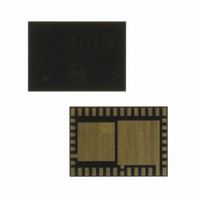
SI1005-C-GM Silicon Laboratories Inc, SI1005-C-GM Datasheet - Page 165

SI1005-C-GM
Manufacturer Part Number
SI1005-C-GM
Description
IC TXRX MCU + EZRADIOPRO
Manufacturer
Silicon Laboratories Inc
Specifications of SI1005-C-GM
Package / Case
42-QFN
Frequency
240MHz ~ 960MHz
Data Rate - Maximum
256kbps
Modulation Or Protocol
FSK, GFSK, OOK
Applications
General Purpose
Power - Output
13dBm
Sensitivity
-121dBm
Voltage - Supply
0.9 V ~ 1.8 V
Current - Receiving
18.5mA
Current - Transmitting
30mA
Data Interface
PCB, Surface Mount
Memory Size
32kB Flash, 4kB RAM
Antenna Connector
PCB, Surface Mount
Number Of Receivers
1
Number Of Transmitters
1
Wireless Frequency
240 MHz to 960 MHz
Interface Type
UART, SMBus, SPI, PCA
Output Power
13 dBm
Operating Supply Voltage
0.9 V to 3.6 V
Maximum Operating Temperature
+ 85 C
Mounting Style
SMD/SMT
Maximum Supply Current
4.1 mA
Minimum Operating Temperature
- 40 C
Modulation
FSK, GFSK, OOK
Protocol Supported
C2, SMBus
Core
8051
Program Memory Type
Flash
Program Memory Size
32 KB
Data Ram Size
4352 B
Supply Current (max)
4.1 mA
Lead Free Status / RoHS Status
Lead free / RoHS Compliant
Operating Temperature
-
Lead Free Status / Rohs Status
Lead free / RoHS Compliant
Other names
336-1875-5
Available stocks
Company
Part Number
Manufacturer
Quantity
Price
Company:
Part Number:
SI1005-C-GM
Manufacturer:
Silicon Labs
Quantity:
135
- Current page: 165 of 376
- Download datasheet (3Mb)
16. On-Chip DC-DC Converter (DC0)
Si1004/5 devices include an on-chip dc-dc converter to allow operation from a single cell battery with a
supply voltage as low as 0.9 V. The dc-dc converter is a switching boost converter with an input voltage
range of 0.9 to 1.8 V and a programmable output voltage range of 1.8 to 3.3 V. The default output voltage
is 1.9 V. The dc-dc converter can supply the system with up to 65 mW of regulated power (or up to
100 mW in some applications) and can be used for powering other devices in the system. This allows the
most flexibility when interfacing to sensors and other analog signals which typically require a higher supply
voltage than a single-cell battery can provide.
Figure 16.1 shows a block diagram of the dc-dc converter. During normal operation in the first half of the
switching cycle, the Duty Cycle Control switch is closed and the Diode Bypass switch is open. Since the
output voltage is higher than the voltage at the DCEN pin, no current flows through the diode and the load
is powered from the output capacitor. During this stage, the DCEN pin is connected to ground through the
Duty Cycle Control switch, generating a positive voltage across the inductor and forcing its current to ramp
up.
In the second half of the switching cycle, the Duty Cycle control switch is opened and the Diode Bypass
switch is closed. This connects DCEN directly to VDD_MCU/DC+ and forces the inductor current to charge
the output capacitor. Once the inductor transfers its stored energy to the output capacitor, the Duty Cycle
Control switch is closed, the Diode Bypass switch is opened, and the cycle repeats.
The dc-dc converter has a built in voltage reference and oscillator, and will automatically limit or turn off the
switching activity in case the peak inductor current rises beyond a safe limit or the output voltage rises
above the programmed target value. This allows the dc-dc converter output to be safely overdriven by a
secondary power source (when available) in order to preserve battery life. The dc-dc converter’s settings
can be modified using SFR registers which provide the ability to change the target output voltage, oscillator
frequency or source, Diode Bypass switch resistance, peak inductor current, and minimum duty cycle.
GND/VBAT-
4.7 uF
0.68 uH
VBAT
DCEN
Figure 16.1. DC-DC Converter Block Diagram
L
Control
Cycle
Duty
parasitic
DC0CN
DC0CF
Bypass
Diode
Rev. 1.0
Control Logic
DC/DC Converter
Reference
Oscillator
Voltage
DC/DC
L
parasitic
Si1000/1/2/3/4/5
GND_MCU/DC-
VDD_MCU/DC+
1uF
I
load
C
load
165
Related parts for SI1005-C-GM
Image
Part Number
Description
Manufacturer
Datasheet
Request
R
Part Number:
Description:
SMD/C°/SINGLE-ENDED OUTPUT SILICON OSCILLATOR
Manufacturer:
Silicon Laboratories Inc
Part Number:
Description:
Manufacturer:
Silicon Laboratories Inc
Datasheet:
Part Number:
Description:
N/A N/A/SI4010 AES KEYFOB DEMO WITH LCD RX
Manufacturer:
Silicon Laboratories Inc
Datasheet:
Part Number:
Description:
N/A N/A/SI4010 SIMPLIFIED KEY FOB DEMO WITH LED RX
Manufacturer:
Silicon Laboratories Inc
Datasheet:
Part Number:
Description:
N/A/-40 TO 85 OC/EZLINK MODULE; F930/4432 HIGH BAND (REV E/B1)
Manufacturer:
Silicon Laboratories Inc
Part Number:
Description:
EZLink Module; F930/4432 Low Band (rev e/B1)
Manufacturer:
Silicon Laboratories Inc
Part Number:
Description:
I°/4460 10 DBM RADIO TEST CARD 434 MHZ
Manufacturer:
Silicon Laboratories Inc
Part Number:
Description:
I°/4461 14 DBM RADIO TEST CARD 868 MHZ
Manufacturer:
Silicon Laboratories Inc
Part Number:
Description:
I°/4463 20 DBM RFSWITCH RADIO TEST CARD 460 MHZ
Manufacturer:
Silicon Laboratories Inc
Part Number:
Description:
I°/4463 20 DBM RADIO TEST CARD 868 MHZ
Manufacturer:
Silicon Laboratories Inc
Part Number:
Description:
I°/4463 27 DBM RADIO TEST CARD 868 MHZ
Manufacturer:
Silicon Laboratories Inc
Part Number:
Description:
I°/4463 SKYWORKS 30 DBM RADIO TEST CARD 915 MHZ
Manufacturer:
Silicon Laboratories Inc
Part Number:
Description:
N/A N/A/-40 TO 85 OC/4463 RFMD 30 DBM RADIO TEST CARD 915 MHZ
Manufacturer:
Silicon Laboratories Inc
Part Number:
Description:
I°/4463 20 DBM RADIO TEST CARD 169 MHZ
Manufacturer:
Silicon Laboratories Inc


