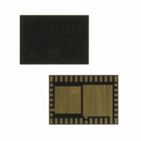
SI1005-C-GM Silicon Laboratories Inc, SI1005-C-GM Datasheet - Page 232

SI1005-C-GM
Manufacturer Part Number
SI1005-C-GM
Description
IC TXRX MCU + EZRADIOPRO
Manufacturer
Silicon Laboratories Inc
Specifications of SI1005-C-GM
Package / Case
42-QFN
Frequency
240MHz ~ 960MHz
Data Rate - Maximum
256kbps
Modulation Or Protocol
FSK, GFSK, OOK
Applications
General Purpose
Power - Output
13dBm
Sensitivity
-121dBm
Voltage - Supply
0.9 V ~ 1.8 V
Current - Receiving
18.5mA
Current - Transmitting
30mA
Data Interface
PCB, Surface Mount
Memory Size
32kB Flash, 4kB RAM
Antenna Connector
PCB, Surface Mount
Number Of Receivers
1
Number Of Transmitters
1
Wireless Frequency
240 MHz to 960 MHz
Interface Type
UART, SMBus, SPI, PCA
Output Power
13 dBm
Operating Supply Voltage
0.9 V to 3.6 V
Maximum Operating Temperature
+ 85 C
Mounting Style
SMD/SMT
Maximum Supply Current
4.1 mA
Minimum Operating Temperature
- 40 C
Modulation
FSK, GFSK, OOK
Protocol Supported
C2, SMBus
Core
8051
Program Memory Type
Flash
Program Memory Size
32 KB
Data Ram Size
4352 B
Supply Current (max)
4.1 mA
Lead Free Status / RoHS Status
Lead free / RoHS Compliant
Operating Temperature
-
Lead Free Status / Rohs Status
Lead free / RoHS Compliant
Other names
336-1875-5
Available stocks
Company
Part Number
Manufacturer
Quantity
Price
Company:
Part Number:
SI1005-C-GM
Manufacturer:
Silicon Labs
Quantity:
135
- Current page: 232 of 376
- Download datasheet (3Mb)
Si1000/1/2/3/4/5
22.4. EZRadioPRO Serial Interface Interrupt Sources
When SPI1 interrupts are enabled, the following flags will generate an interrupt when they are set to logic
1:
All of the following bits must be cleared by software.
22.5. Serial Clock Phase and Polarity
Four combinations of serial clock phase and polarity can be selected using the clock control bits in the SPI
Configuration Register (SPI1CFG). The CKPHA bit (SPI1CFG.5) selects one of two clock phases (edge
used to latch the data). The CKPOL bit (SPI1CFG.4) selects between an active-high or active-low clock.
Both CKPOL and CKPHA must be set to zero in order to communicate with the EZRadioPRO peripheral.
The SPI1 Clock Rate Register (SPI1CKR) as shown in SFR Definition 22.3 controls the master mode
serial clock frequency. When the SPI is configured as a master, the maximum data transfer rate (bits/sec)
is one-half the system clock frequency or 12.5 MHz, whichever is slower.
232
NSS (Must Remain High
in Multi-Master Mode)
SCK
(CKPOL=0, CKPHA=0)
SCK
(CKPOL=0, CKPHA=1)
SCK
(CKPOL=1, CKPHA=0)
SCK
(CKPOL=1, CKPHA=1)
MISO/MOSI
1. The SPI Interrupt Flag, SPIFn (SPInCN.7) is set to logic 1 at the end of each byte transfer.
2. The Write Collision Flag, WCOLn (SPInCN.6) is set to logic 1 if a write to SPInDAT is
3. The Mode Fault Flag MODFn (SPInCN.5) is set to logic 1 when SPIn is configured as a
4. The Receive Overrun Flag RXOVRNn (SPInCN.4) is set to logic 1 when configured as a slave,
This flag can occur in all SPIn modes.
attempted when the transmit buffer has not been emptied to the SPI shift register. When this
occurs, the write to SPInDAT will be ignored, and the transmit buffer will not be written.This
flag can occur in all SPIn modes.
master, and for multi-master mode and the NSS pin is pulled low. When a Mode Fault occurs,
the MSTENn and SPIENn bits in SPI0CN are set to logic 0 to disable SPIn and allow another
master device to access the bus.
and a transfer is completed and the receive buffer still holds an unread byte from a previous
transfer. The new byte is not transferred to the receive buffer, allowing the previously received
data byte to be read. The data byte which caused the overrun is lost.
Figure 22.6. Master Mode Data/Clock Timing
MSB
Bit 6
Bit 5
Rev. 1.0
Bit 4
Bit 3
Bit 2
Bit 1
Bit 0
Related parts for SI1005-C-GM
Image
Part Number
Description
Manufacturer
Datasheet
Request
R
Part Number:
Description:
SMD/C°/SINGLE-ENDED OUTPUT SILICON OSCILLATOR
Manufacturer:
Silicon Laboratories Inc
Part Number:
Description:
Manufacturer:
Silicon Laboratories Inc
Datasheet:
Part Number:
Description:
N/A N/A/SI4010 AES KEYFOB DEMO WITH LCD RX
Manufacturer:
Silicon Laboratories Inc
Datasheet:
Part Number:
Description:
N/A N/A/SI4010 SIMPLIFIED KEY FOB DEMO WITH LED RX
Manufacturer:
Silicon Laboratories Inc
Datasheet:
Part Number:
Description:
N/A/-40 TO 85 OC/EZLINK MODULE; F930/4432 HIGH BAND (REV E/B1)
Manufacturer:
Silicon Laboratories Inc
Part Number:
Description:
EZLink Module; F930/4432 Low Band (rev e/B1)
Manufacturer:
Silicon Laboratories Inc
Part Number:
Description:
I°/4460 10 DBM RADIO TEST CARD 434 MHZ
Manufacturer:
Silicon Laboratories Inc
Part Number:
Description:
I°/4461 14 DBM RADIO TEST CARD 868 MHZ
Manufacturer:
Silicon Laboratories Inc
Part Number:
Description:
I°/4463 20 DBM RFSWITCH RADIO TEST CARD 460 MHZ
Manufacturer:
Silicon Laboratories Inc
Part Number:
Description:
I°/4463 20 DBM RADIO TEST CARD 868 MHZ
Manufacturer:
Silicon Laboratories Inc
Part Number:
Description:
I°/4463 27 DBM RADIO TEST CARD 868 MHZ
Manufacturer:
Silicon Laboratories Inc
Part Number:
Description:
I°/4463 SKYWORKS 30 DBM RADIO TEST CARD 915 MHZ
Manufacturer:
Silicon Laboratories Inc
Part Number:
Description:
N/A N/A/-40 TO 85 OC/4463 RFMD 30 DBM RADIO TEST CARD 915 MHZ
Manufacturer:
Silicon Laboratories Inc
Part Number:
Description:
I°/4463 20 DBM RADIO TEST CARD 169 MHZ
Manufacturer:
Silicon Laboratories Inc


