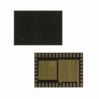
SI1005-C-GM Silicon Laboratories Inc, SI1005-C-GM Datasheet - Page 74

SI1005-C-GM
Manufacturer Part Number
SI1005-C-GM
Description
IC TXRX MCU + EZRADIOPRO
Manufacturer
Silicon Laboratories Inc
Specifications of SI1005-C-GM
Package / Case
42-QFN
Frequency
240MHz ~ 960MHz
Data Rate - Maximum
256kbps
Modulation Or Protocol
FSK, GFSK, OOK
Applications
General Purpose
Power - Output
13dBm
Sensitivity
-121dBm
Voltage - Supply
0.9 V ~ 1.8 V
Current - Receiving
18.5mA
Current - Transmitting
30mA
Data Interface
PCB, Surface Mount
Memory Size
32kB Flash, 4kB RAM
Antenna Connector
PCB, Surface Mount
Number Of Receivers
1
Number Of Transmitters
1
Wireless Frequency
240 MHz to 960 MHz
Interface Type
UART, SMBus, SPI, PCA
Output Power
13 dBm
Operating Supply Voltage
0.9 V to 3.6 V
Maximum Operating Temperature
+ 85 C
Mounting Style
SMD/SMT
Maximum Supply Current
4.1 mA
Minimum Operating Temperature
- 40 C
Modulation
FSK, GFSK, OOK
Protocol Supported
C2, SMBus
Core
8051
Program Memory Type
Flash
Program Memory Size
32 KB
Data Ram Size
4352 B
Supply Current (max)
4.1 mA
Lead Free Status / RoHS Status
Lead free / RoHS Compliant
Operating Temperature
-
Lead Free Status / Rohs Status
Lead free / RoHS Compliant
Other names
336-1875-5
Available stocks
Company
Part Number
Manufacturer
Quantity
Price
Company:
Part Number:
SI1005-C-GM
Manufacturer:
Silicon Labs
Quantity:
135
- Current page: 74 of 376
- Download datasheet (3Mb)
Si1000/1/2/3/4/5
5. 10-Bit SAR ADC with 16-bit Auto-Averaging Accumulator and
The ADC0 on the Si1000/1/2/3/4/5 is a 300 ksps, 10-bit successive-approximation-register (SAR) ADC
with integrated track-and-hold and programmable window detector. ADC0 also has an autonomous low
power Burst Mode which can automatically enable ADC0, capture and accumulate samples, then place
ADC0 in a low power shutdown mode without CPU intervention. It also has a 16-bit accumulator that can
automatically oversample and average the ADC results.
The ADC is fully configurable under software control via Special Function Registers. The ADC0 operates in
Single-ended mode and may be configured to measure various different signals using the analog multi-
plexer described in “5.5. ADC0 Analog Multiplexer” on page 90. The voltage reference for the ADC is
selected as described in “5.7. Voltage and Ground Reference Options” on page 95.
5.1. Output Code Formatting
The registers ADC0H and ADC0L contain the high and low bytes of the output conversion code from the
ADC at the completion of each conversion. Data can be right-justified or left-justified, depending on the
setting of the AD0SJST[2:0]. When the repeat count is set to 1, conversion codes are represented as 10-
bit unsigned integers. Inputs are measured from 0 to VREF x 1023/1024. Example codes are shown below
for both right-justified and left-justified data. Unused bits in the ADC0H and ADC0L registers are set to 0.
74
Autonomous Low Power Burst Mode
ADC0PWR
ADC0TK
AMUX0
From
Burst Mode Logic
AIN+
Figure 5.1. ADC0 Functional Block Diagram
ADC0CF
ADC
10-bit
VDD
SAR
ADC0GTH ADC0GTL
ADC0LTH
Rev. 1.0
ADC0CN
ADC0LTL
Conversion
Start
100
000
001
010
011
32
16-Bit Accumulator
AD0WINT
Compare
W indow
CNVSTR Input
AD0BUSY (W )
Timer 0 Overflow
Timer 2 Overflow
Timer 3 Overflow
Logic
Related parts for SI1005-C-GM
Image
Part Number
Description
Manufacturer
Datasheet
Request
R
Part Number:
Description:
SMD/C°/SINGLE-ENDED OUTPUT SILICON OSCILLATOR
Manufacturer:
Silicon Laboratories Inc
Part Number:
Description:
Manufacturer:
Silicon Laboratories Inc
Datasheet:
Part Number:
Description:
N/A N/A/SI4010 AES KEYFOB DEMO WITH LCD RX
Manufacturer:
Silicon Laboratories Inc
Datasheet:
Part Number:
Description:
N/A N/A/SI4010 SIMPLIFIED KEY FOB DEMO WITH LED RX
Manufacturer:
Silicon Laboratories Inc
Datasheet:
Part Number:
Description:
N/A/-40 TO 85 OC/EZLINK MODULE; F930/4432 HIGH BAND (REV E/B1)
Manufacturer:
Silicon Laboratories Inc
Part Number:
Description:
EZLink Module; F930/4432 Low Band (rev e/B1)
Manufacturer:
Silicon Laboratories Inc
Part Number:
Description:
I°/4460 10 DBM RADIO TEST CARD 434 MHZ
Manufacturer:
Silicon Laboratories Inc
Part Number:
Description:
I°/4461 14 DBM RADIO TEST CARD 868 MHZ
Manufacturer:
Silicon Laboratories Inc
Part Number:
Description:
I°/4463 20 DBM RFSWITCH RADIO TEST CARD 460 MHZ
Manufacturer:
Silicon Laboratories Inc
Part Number:
Description:
I°/4463 20 DBM RADIO TEST CARD 868 MHZ
Manufacturer:
Silicon Laboratories Inc
Part Number:
Description:
I°/4463 27 DBM RADIO TEST CARD 868 MHZ
Manufacturer:
Silicon Laboratories Inc
Part Number:
Description:
I°/4463 SKYWORKS 30 DBM RADIO TEST CARD 915 MHZ
Manufacturer:
Silicon Laboratories Inc
Part Number:
Description:
N/A N/A/-40 TO 85 OC/4463 RFMD 30 DBM RADIO TEST CARD 915 MHZ
Manufacturer:
Silicon Laboratories Inc
Part Number:
Description:
I°/4463 20 DBM RADIO TEST CARD 169 MHZ
Manufacturer:
Silicon Laboratories Inc


