DK-DEV-5M570ZN Altera, DK-DEV-5M570ZN Datasheet - Page 109
DK-DEV-5M570ZN
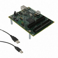
Manufacturer Part Number
DK-DEV-5M570ZN
Description
KIT DEV MAX V 5M570Z
Manufacturer
Altera
Series
MAX® Vr
Type
CPLDr
Datasheets
1.DK-DEV-5M570ZN.pdf
(30 pages)
2.DK-DEV-5M570ZN.pdf
(2 pages)
3.DK-DEV-5M570ZN.pdf
(30 pages)
4.DK-DEV-5M570ZN.pdf
(164 pages)
5.DK-DEV-5M570ZN.pdf
(24 pages)
Specifications of DK-DEV-5M570ZN
Contents
Board, Cable(s), Software and Documentation
Silicon Manufacturer
Altera
Core Architecture
CPLD
Core Sub-architecture
MAX
Silicon Core Number
5M
Silicon Family Name
MAX V
Kit Contents
MAX V CPLD Development Board, USB Cable
Rohs Compliant
Yes
Lead Free Status / RoHS Status
Lead free / RoHS Compliant
For Use With/related Products
5M570ZF256
Lead Free Status / Rohs Status
Compliant
Other names
544-2722
Available stocks
Company
Part Number
Manufacturer
Quantity
Price


Chapter 7: User Flash Memory in MAX V Devices
UFM Functional Description
January 2011 Altera Corporation
Oscillator
1
1
OSC_ENA, one of the input signals in the UFM block, is used to enable the oscillator
signal to output through the OSC output port. You can use this OSC output port to
connect with the interface logic in the logic array. It can be routed through the logic
array and fed back as an input clock for the address register (ARCLK) and the data
register (DRCLK). The output frequency of the OSC port is one-fourth that of the
oscillator frequency. As a result, the frequency range of the OSC port is 3.9 to 5.3 MHz.
The maximum clock frequency accepted by ARCLK and DRCLK is 10 MHz and the duty
cycle accepted by the DRCLK and ARCLK input ports is approximately 45% to 50%.
When the OSC_ENA input signal is asserted, the oscillator is enabled and the output is
routed to the logic array through the OSC output. When the OSC_ENA signal is set low,
the OSC output drives constant high. The routing delay from the OSC port of the UFM
block to OSC output pin depends on placement. You can analyze this delay using the
TimeQuest timing analyzer.
The undivided internal oscillator, which is not accessible, operates in a frequency
range from 15.6 to 21.2 MHz. The internal oscillator is enabled during power-up,
in-system programming, and real-time ISP. At all other times, the oscillator is not
running unless the UFM is instantiated in the design and the OSC_ENA port is asserted.
To see how specific operating modes of the ALTUFM megafunction handle OSC_ENA
and the oscillator, refer to
generated logic interfacing to the UFM, the oscillator must be enabled during
program or erase operations, but not during read operations. The OSC_ENA signal can
be tied low if you are not issuing any PROGRAM or ERASE commands.
During real-time ISP operation, the internal oscillator automatically enables and
outputs through the OSC output port (if this port is instantiated) even though the
OSC_ENA signal is tied low. You can use the RTP_BUSY signal to detect the beginning and
ending of the real-time ISP operation for gated control of this self-enabled OSC output
condition.
The internal oscillator is not enabled all the time. The internal oscillator for the
program or erase operation is only activated when the flash memory block is being
programmed or erased. During a read operation, the internal oscillator is activated
whenever the flash memory block is reading data.
Instantiating the Oscillator without the UFM
You can use the MAX II/MAX V Oscillator megafunction selection in the
MegaWizard
this signal without using the UFM memory block.
ALTUFM_OSC megafunction instantiation in the Quartus II software.
Figure 7–4. The Quartus II ALTUFM_OSC Megafunction
™
Plug-In Manager to instantiate the UFM oscillator if you intend to use
“Software Support for UFM Block” on page
Figure 7–4
shows the
MAX V Device Handbook
7–13. For user-
7–7
Related parts for DK-DEV-5M570ZN
Image
Part Number
Description
Manufacturer
Datasheet
Request
R

Part Number:
Description:
KIT DEV ARRIA II GX FPGA 2AGX125
Manufacturer:
Altera
Datasheet:

Part Number:
Description:
KIT DEV CYCLONE III LS EP3CLS200
Manufacturer:
Altera
Datasheet:

Part Number:
Description:
KIT DEV STRATIX IV FPGA 4SE530
Manufacturer:
Altera
Datasheet:

Part Number:
Description:
KIT DEV FPGA 2AGX260 W/6.375G TX
Manufacturer:
Altera
Datasheet:

Part Number:
Description:
KIT DEV STRATIX V FPGA 5SGXEA7
Manufacturer:
Altera
Datasheet:

Part Number:
Description:
KIT DEVELOPMENT STRATIX III
Manufacturer:
Altera
Datasheet:

Part Number:
Description:
KIT DEVELOPMENT STRATIX IV
Manufacturer:
Altera
Datasheet:

Part Number:
Description:
KIT DEV ARRIA GX 1AGX60N
Manufacturer:
Altera
Datasheet:
Part Number:
Description:
KIT STARTER CYCLONE IV GX
Manufacturer:
Altera
Datasheet:
Part Number:
Description:
KIT DEVELOPMENT STRATIX IV
Manufacturer:
Altera
Datasheet:

Part Number:
Description:
CPLD, EP610 Family, ECMOS Process, 300 Gates, 16 Macro Cells, 16 Reg., 16 User I/Os, 5V Supply, 35 Speed Grade, 24DIP
Manufacturer:
Altera Corporation
Datasheet:
Part Number:
Description:
CPLD, EP610 Family, ECMOS Process, 300 Gates, 16 Macro Cells, 16 Reg., 16 User I/Os, 5V Supply, 15 Speed Grade, 24DIP
Manufacturer:
Altera Corporation
Datasheet: