DK-DEV-5M570ZN Altera, DK-DEV-5M570ZN Datasheet - Page 116
DK-DEV-5M570ZN
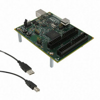
Manufacturer Part Number
DK-DEV-5M570ZN
Description
KIT DEV MAX V 5M570Z
Manufacturer
Altera
Series
MAX® Vr
Type
CPLDr
Datasheets
1.DK-DEV-5M570ZN.pdf
(30 pages)
2.DK-DEV-5M570ZN.pdf
(2 pages)
3.DK-DEV-5M570ZN.pdf
(30 pages)
4.DK-DEV-5M570ZN.pdf
(164 pages)
5.DK-DEV-5M570ZN.pdf
(24 pages)
Specifications of DK-DEV-5M570ZN
Contents
Board, Cable(s), Software and Documentation
Silicon Manufacturer
Altera
Core Architecture
CPLD
Core Sub-architecture
MAX
Silicon Core Number
5M
Silicon Family Name
MAX V
Kit Contents
MAX V CPLD Development Board, USB Cable
Rohs Compliant
Yes
Lead Free Status / RoHS Status
Lead free / RoHS Compliant
For Use With/related Products
5M570ZF256
Lead Free Status / Rohs Status
Compliant
Other names
544-2722
Available stocks
Company
Part Number
Manufacturer
Quantity
Price


7–14
Table 7–5. ALTUFM_I2C Interface Signals
Figure 7–9. Start and Stop Conditions
MAX V Device Handbook
SDA
SCL
WP
A
2
, A
Pin
1
, A
0
SDA
SCL
Serial Data/Address Line
Serial Clock Line
Write Protect
Slave Address Input
Start Condition
Description
■
■
■
Table 7–5
START and STOP Condition
The master always generates start (S) and stop (P) conditions. After the start
condition, the bus is considered busy. Only a stop (P) condition frees the bus. The bus
stays busy if the repeated start (Sr) condition is executed instead of a stop condition.
In this occurrence, the start (S) and repeated start (Sr) conditions are functionally
identical.
A high-to-low transition on the SDA line while the SCL is high indicates a start
condition. A low-to-high transition on the SDA line while the SCL is high indicates a
stop condition.
S
Data transfer can be initiated only when the bus is free.
The data on the SDA line must be stable during the high period of the clock. The
high or low state of the data line can only change when the clock signal on the SCL
line is low.
Any transition on the SDA line while the SCL is high indicates a start or stop
condition.
lists the ALTUFM_I2C megafunction input and output interface signals.
Figure 7–9
The bidirectional SDA port is used to transmit and receive serial data from the
UFM. The output stage of the SDA port is configured as an open drain pin to
perform the wired-AND function.
The bidirectional SCL port is used to synchronize the serial data transfer to and
from the UFM. The output stage of the SCL port is configured as an open drain
pin to perform a wired-AND function.
Optional active high signal that disables the erase and write function for
read/write mode. The ALTUFM_I2C megafunction gives you an option to
protect the entire UFM memory or only the upper half of memory.
These inputs set the UFM slave address. The A
are programmable, set internally to 1010 by default.
shows the start and stop conditions.
Function
Chapter 7: User Flash Memory in MAX V Devices
Stop Condition
6
, A
5
January 2011 Altera Corporation
P
, A
Software Support for UFM Block
4
, A
3
slave address bits
SDA
SCL
Related parts for DK-DEV-5M570ZN
Image
Part Number
Description
Manufacturer
Datasheet
Request
R

Part Number:
Description:
KIT DEV ARRIA II GX FPGA 2AGX125
Manufacturer:
Altera
Datasheet:

Part Number:
Description:
KIT DEV CYCLONE III LS EP3CLS200
Manufacturer:
Altera
Datasheet:

Part Number:
Description:
KIT DEV STRATIX IV FPGA 4SE530
Manufacturer:
Altera
Datasheet:

Part Number:
Description:
KIT DEV FPGA 2AGX260 W/6.375G TX
Manufacturer:
Altera
Datasheet:

Part Number:
Description:
KIT DEV STRATIX V FPGA 5SGXEA7
Manufacturer:
Altera
Datasheet:

Part Number:
Description:
KIT DEVELOPMENT STRATIX III
Manufacturer:
Altera
Datasheet:

Part Number:
Description:
KIT DEVELOPMENT STRATIX IV
Manufacturer:
Altera
Datasheet:

Part Number:
Description:
KIT DEV ARRIA GX 1AGX60N
Manufacturer:
Altera
Datasheet:
Part Number:
Description:
KIT STARTER CYCLONE IV GX
Manufacturer:
Altera
Datasheet:
Part Number:
Description:
KIT DEVELOPMENT STRATIX IV
Manufacturer:
Altera
Datasheet:

Part Number:
Description:
CPLD, EP610 Family, ECMOS Process, 300 Gates, 16 Macro Cells, 16 Reg., 16 User I/Os, 5V Supply, 35 Speed Grade, 24DIP
Manufacturer:
Altera Corporation
Datasheet:
Part Number:
Description:
CPLD, EP610 Family, ECMOS Process, 300 Gates, 16 Macro Cells, 16 Reg., 16 User I/Os, 5V Supply, 15 Speed Grade, 24DIP
Manufacturer:
Altera Corporation
Datasheet: