DK-DEV-5M570ZN Altera, DK-DEV-5M570ZN Datasheet - Page 136
DK-DEV-5M570ZN
Manufacturer Part Number
DK-DEV-5M570ZN
Description
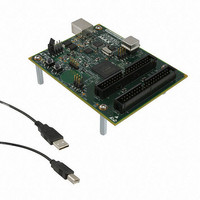
KIT DEV MAX V 5M570Z
Manufacturer
Altera
Series
MAX® Vr
Type
CPLDr
Datasheets
1.DK-DEV-5M570ZN.pdf
(30 pages)
2.DK-DEV-5M570ZN.pdf
(2 pages)
3.DK-DEV-5M570ZN.pdf
(30 pages)
4.DK-DEV-5M570ZN.pdf
(164 pages)
5.DK-DEV-5M570ZN.pdf
(24 pages)
Specifications of DK-DEV-5M570ZN
Contents
Board, Cable(s), Software and Documentation
Silicon Manufacturer
Altera
Core Architecture
CPLD
Core Sub-architecture
MAX
Silicon Core Number
5M
Silicon Family Name
MAX V
Kit Contents
MAX V CPLD Development Board, USB Cable
Rohs Compliant
Yes
Lead Free Status / RoHS Status
Lead free / RoHS Compliant
For Use With/related Products
5M570ZF256
Lead Free Status / Rohs Status
Compliant
Other names
544-2722
Available stocks
Company
Part Number
Manufacturer
Quantity
Price


7–34
MAX V Device Handbook
WRSR (Write Status Register)
The block protection bits(BP1 and BP0) are the status bits used to protect certain
sections of the UFM from inadvertent write. The BP1 and BP0 status are updated by
WRSR. During WRSR, only BP1 and BP0 in the status register can be written with valid
information. The rest of the bits in the status register are ignored and not updated.
When both BP1 and BP0 are 0, there is no protection for the UFM. When both BP1 and
BP0 are 1, there is full protection for the UFM. BP0 and BP1 are set to 0 upon power-up.
Table 7–12
the Block Write Protect Bits for Base mode. WRSR is issued through the following
sequence, as shown in
1. nCS is pulled low.
2. Opcode 00000001 is transmitted into the interface.
3. An 8-bit status is transmitted into the interface to update BP1 and BP0 of the status
4. If nCS is pulled high too early (before all the eight bits in Step 2 or Step 3 are
5. nCS is pulled back to high to terminate the transmission.
Figure 7–31. WRSR Operation Sequence
Table 7–12. Block Write Protect Bits for Extended Mode
Table 7–13. Block Write Protect Bits for Base Mode
0 (No protection)
3 (Full protection)
0 (No protection)
3 (Full protection)
register.
transmitted) or too late (the ninth bit or more is transmitted), WRSR is not executed.
Level
Level
lists the Block Write Protect Bits for Extended mode, while
SCK
nCS
SI
SO
Figure
MSB
BP1
BP1
7–31:
Status Register Bits
Status Register Bits
0
0
1
0
1
1
Instruction
2
8-bit
01
3
H
4
High Impedance
5 6 7
BP0
BP0
0
1
0
1
MSB
8
Status Register In
9 10 11 12 13 14 15
Chapter 7: User Flash Memory in MAX V Devices
UFM Array Address
UFM Array Address
000 to 1FF
000 to 0FF
Protected
Protected
January 2011 Altera Corporation
None
None
Software Support for UFM Block
Table 7–13
lists
Related parts for DK-DEV-5M570ZN
Image
Part Number
Description
Manufacturer
Datasheet
Request
R

Part Number:
Description:
KIT DEV ARRIA II GX FPGA 2AGX125
Manufacturer:
Altera
Datasheet:

Part Number:
Description:
KIT DEV CYCLONE III LS EP3CLS200
Manufacturer:
Altera
Datasheet:

Part Number:
Description:
KIT DEV STRATIX IV FPGA 4SE530
Manufacturer:
Altera
Datasheet:

Part Number:
Description:
KIT DEV FPGA 2AGX260 W/6.375G TX
Manufacturer:
Altera
Datasheet:

Part Number:
Description:
KIT DEV STRATIX V FPGA 5SGXEA7
Manufacturer:
Altera
Datasheet:

Part Number:
Description:
KIT DEVELOPMENT STRATIX III
Manufacturer:
Altera
Datasheet:

Part Number:
Description:
KIT DEVELOPMENT STRATIX IV
Manufacturer:
Altera
Datasheet:

Part Number:
Description:
KIT DEV ARRIA GX 1AGX60N
Manufacturer:
Altera
Datasheet:
Part Number:
Description:
KIT STARTER CYCLONE IV GX
Manufacturer:
Altera
Datasheet:
Part Number:
Description:
KIT DEVELOPMENT STRATIX IV
Manufacturer:
Altera
Datasheet:

Part Number:
Description:
CPLD, EP610 Family, ECMOS Process, 300 Gates, 16 Macro Cells, 16 Reg., 16 User I/Os, 5V Supply, 35 Speed Grade, 24DIP
Manufacturer:
Altera Corporation
Datasheet:
Part Number:
Description:
CPLD, EP610 Family, ECMOS Process, 300 Gates, 16 Macro Cells, 16 Reg., 16 User I/Os, 5V Supply, 15 Speed Grade, 24DIP
Manufacturer:
Altera Corporation
Datasheet: