DK-DEV-5M570ZN Altera, DK-DEV-5M570ZN Datasheet - Page 127
DK-DEV-5M570ZN
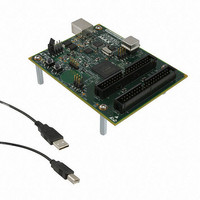
Manufacturer Part Number
DK-DEV-5M570ZN
Description
KIT DEV MAX V 5M570Z
Manufacturer
Altera
Series
MAX® Vr
Type
CPLDr
Datasheets
1.DK-DEV-5M570ZN.pdf
(30 pages)
2.DK-DEV-5M570ZN.pdf
(2 pages)
3.DK-DEV-5M570ZN.pdf
(30 pages)
4.DK-DEV-5M570ZN.pdf
(164 pages)
5.DK-DEV-5M570ZN.pdf
(24 pages)
Specifications of DK-DEV-5M570ZN
Contents
Board, Cable(s), Software and Documentation
Silicon Manufacturer
Altera
Core Architecture
CPLD
Core Sub-architecture
MAX
Silicon Core Number
5M
Silicon Family Name
MAX V
Kit Contents
MAX V CPLD Development Board, USB Cable
Rohs Compliant
Yes
Lead Free Status / RoHS Status
Lead free / RoHS Compliant
For Use With/related Products
5M570ZF256
Lead Free Status / Rohs Status
Compliant
Other names
544-2722
Available stocks
Company
Part Number
Manufacturer
Quantity
Price


Chapter 7: User Flash Memory in MAX V Devices
Software Support for UFM Block
Table 7–11. Status Register Format
January 2011 Altera Corporation
Bit 7
Bit 6
Bit 5
Bit 4
Bit 3
Bit 2
Bit 1
Bit 0
Note to
(1) For more information about status register bits BP1 and BP0, refer to
Position
Table
7–11:
Status
nRDY
WEN
BP1
BP0
X
X
X
X
Opcodes
Table 7–10
opcode must be provided. Otherwise, the interface assumes that the master device
has internal logic errors and ignores the rest of the incoming signals. When nCS is
pulled back to high, the interface is back to normal. nCS should be pulled low again
for a new service request.
Table 7–10. Instruction Set for SPI
The READ and WRITE opcodes are instructions for transmission, which means the data
will be read from or written to the UFM.
WREN, WRDI, RDSR, and WRSR are instructions for the status register, where they do not
have any direct interaction with UFM, but read or set the status register within the
interface logic. The status register provides status on whether the UFM block is
available for any READ or WRITE operation, whether the interface is WRITE enabled, and
the state of the UFM WRITE protection.
the read only implementation of ALTUFM SPI (Base or Extended mode), the status
register does not exist, saving LE resources.
The following sections describe the instructions for SPI.
WREN
WRDI
RDSR
WRSR
READ
WRITE
SECTOR-ERASE
UFM-ERASE
Name
Default at Power-Up
lists the 8-bit instruction opcodes. After nCS is pulled low, the indicated
0
0
0
0
0
0
0
0
00000110
00000100
00000101
00000001
00000011
00000010
00100000
01100000
Opcode
Table 7–12
Indicate the current level of block write protection
Indicate the current level of block write protection
1 = Busy, UFM WRITE or ERASE cycle in progress
0 = No UFM WRITE or ERASE cycle in progress
Table 7–11
Enable Write to UFM
Disable Write to UFM
Read Status Register
Write Status Register
Read data from UFM
Write data to UFM
Sector erase
Erase the entire UFM block (both sectors)
and
Table 7–13 on page
0= SPI WRITE disabled state
1= SPI WRITE enabled state
lists the status register format. For
Description
—
—
—
—
Operation
7–34.
MAX V Device Handbook
(1)
(1)
7–25
Related parts for DK-DEV-5M570ZN
Image
Part Number
Description
Manufacturer
Datasheet
Request
R

Part Number:
Description:
KIT DEV ARRIA II GX FPGA 2AGX125
Manufacturer:
Altera
Datasheet:

Part Number:
Description:
KIT DEV CYCLONE III LS EP3CLS200
Manufacturer:
Altera
Datasheet:

Part Number:
Description:
KIT DEV STRATIX IV FPGA 4SE530
Manufacturer:
Altera
Datasheet:

Part Number:
Description:
KIT DEV FPGA 2AGX260 W/6.375G TX
Manufacturer:
Altera
Datasheet:

Part Number:
Description:
KIT DEV STRATIX V FPGA 5SGXEA7
Manufacturer:
Altera
Datasheet:

Part Number:
Description:
KIT DEVELOPMENT STRATIX III
Manufacturer:
Altera
Datasheet:

Part Number:
Description:
KIT DEVELOPMENT STRATIX IV
Manufacturer:
Altera
Datasheet:

Part Number:
Description:
KIT DEV ARRIA GX 1AGX60N
Manufacturer:
Altera
Datasheet:
Part Number:
Description:
KIT STARTER CYCLONE IV GX
Manufacturer:
Altera
Datasheet:
Part Number:
Description:
KIT DEVELOPMENT STRATIX IV
Manufacturer:
Altera
Datasheet:

Part Number:
Description:
CPLD, EP610 Family, ECMOS Process, 300 Gates, 16 Macro Cells, 16 Reg., 16 User I/Os, 5V Supply, 35 Speed Grade, 24DIP
Manufacturer:
Altera Corporation
Datasheet:
Part Number:
Description:
CPLD, EP610 Family, ECMOS Process, 300 Gates, 16 Macro Cells, 16 Reg., 16 User I/Os, 5V Supply, 15 Speed Grade, 24DIP
Manufacturer:
Altera Corporation
Datasheet: