DK-DEV-5M570ZN Altera, DK-DEV-5M570ZN Datasheet - Page 21
DK-DEV-5M570ZN
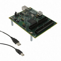
Manufacturer Part Number
DK-DEV-5M570ZN
Description
KIT DEV MAX V 5M570Z
Manufacturer
Altera
Series
MAX® Vr
Type
CPLDr
Datasheets
1.DK-DEV-5M570ZN.pdf
(30 pages)
2.DK-DEV-5M570ZN.pdf
(2 pages)
3.DK-DEV-5M570ZN.pdf
(30 pages)
4.DK-DEV-5M570ZN.pdf
(164 pages)
5.DK-DEV-5M570ZN.pdf
(24 pages)
Specifications of DK-DEV-5M570ZN
Contents
Board, Cable(s), Software and Documentation
Silicon Manufacturer
Altera
Core Architecture
CPLD
Core Sub-architecture
MAX
Silicon Core Number
5M
Silicon Family Name
MAX V
Kit Contents
MAX V CPLD Development Board, USB Cable
Rohs Compliant
Yes
Lead Free Status / RoHS Status
Lead free / RoHS Compliant
For Use With/related Products
5M570ZF256
Lead Free Status / Rohs Status
Compliant
Other names
544-2722
Available stocks
Company
Part Number
Manufacturer
Quantity
Price


Chapter 2: MAX V Architecture
Logic Elements
December 2010 Altera Corporation
LUT Chain and Register Chain
addnsub Signal
LE Operating Modes
improves device utilization because the device can use the register and the LUT for
unrelated functions. Another special packing mode allows the register output to feed
back into the LUT of the same LE so that the register is packed with its own fan-out
LUT. This mode provides another mechanism for improved fitting. The LE can also
drive out registered and unregistered versions of the LUT output.
In addition to the three general routing outputs, the LEs within a LAB have LUT chain
and register chain outputs. LUT chain connections allow LUTs within the same LAB
to cascade together for wide input functions. Register chain outputs allow registers
within the same LAB to cascade together. The register chain output allows a LAB to
use LUTs for a single combinational function and the registers for an unrelated shift
register implementation. These resources speed up connections between LABs while
saving local interconnect resources. For more information about LUT chain and
register chain connections, refer to
The LE’s dynamic adder/subtractor feature saves logic resources by using one set of
LEs to implement both an adder and a subtractor. This feature is controlled by the
LAB-wide control signal addnsub. The addnsub signal sets the LAB to perform either
A + B or A – B. The LUT computes addition; subtraction is computed by adding the
two’s complement of the intended subtractor. The LAB-wide signal converts to two’s
complement by inverting the B bits within the LAB and setting carry-in to 1, which
adds one to the LSB. The LSB of an adder/subtractor must be placed in the first LE of
the LAB, where the LAB-wide addnsub signal automatically sets the carry-in to 1. The
Quartus II Compiler automatically places and uses the adder/subtractor feature
when using adder/subtractor parameterized functions.
The MAX V LE can operate in one of the following modes:
■
■
Each mode uses LE resources differently. In each mode, eight available inputs to the
LE, the four data inputs from the LAB local interconnect, carry-in0 and carry-in1
from the previous LE, the LAB carry-in from the previous carry-chain LAB, and the
register chain connection are directed to different destinations to implement the
desired logic function. LAB-wide signals provide clock, asynchronous clear,
asynchronous preset/load, synchronous clear, synchronous load, and clock enable
control for the register. These LAB-wide signals are available in all LE modes. The
addnsub control signal is allowed in arithmetic mode.
The Quartus II software, along with parameterized functions such as the library of
parameterized modules (LPM) functions, automatically chooses the appropriate
mode for common functions such as counters, adders, subtractors, and arithmetic
functions.
“Normal Mode”
“Dynamic Arithmetic Mode”
“MultiTrack Interconnect” on page
MAX V Device Handbook
2–14.
2–9
Related parts for DK-DEV-5M570ZN
Image
Part Number
Description
Manufacturer
Datasheet
Request
R

Part Number:
Description:
KIT DEV ARRIA II GX FPGA 2AGX125
Manufacturer:
Altera
Datasheet:

Part Number:
Description:
KIT DEV CYCLONE III LS EP3CLS200
Manufacturer:
Altera
Datasheet:

Part Number:
Description:
KIT DEV STRATIX IV FPGA 4SE530
Manufacturer:
Altera
Datasheet:

Part Number:
Description:
KIT DEV FPGA 2AGX260 W/6.375G TX
Manufacturer:
Altera
Datasheet:

Part Number:
Description:
KIT DEV STRATIX V FPGA 5SGXEA7
Manufacturer:
Altera
Datasheet:

Part Number:
Description:
KIT DEVELOPMENT STRATIX III
Manufacturer:
Altera
Datasheet:

Part Number:
Description:
KIT DEVELOPMENT STRATIX IV
Manufacturer:
Altera
Datasheet:

Part Number:
Description:
KIT DEV ARRIA GX 1AGX60N
Manufacturer:
Altera
Datasheet:
Part Number:
Description:
KIT STARTER CYCLONE IV GX
Manufacturer:
Altera
Datasheet:
Part Number:
Description:
KIT DEVELOPMENT STRATIX IV
Manufacturer:
Altera
Datasheet:

Part Number:
Description:
CPLD, EP610 Family, ECMOS Process, 300 Gates, 16 Macro Cells, 16 Reg., 16 User I/Os, 5V Supply, 35 Speed Grade, 24DIP
Manufacturer:
Altera Corporation
Datasheet:
Part Number:
Description:
CPLD, EP610 Family, ECMOS Process, 300 Gates, 16 Macro Cells, 16 Reg., 16 User I/Os, 5V Supply, 15 Speed Grade, 24DIP
Manufacturer:
Altera Corporation
Datasheet: