ATMEGA168PA-PU Atmel, ATMEGA168PA-PU Datasheet - Page 137
ATMEGA168PA-PU
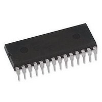
Manufacturer Part Number
ATMEGA168PA-PU
Description
MCU, 8BIT, AVR, 16K FLASH, 28PDIP
Manufacturer
Atmel
Datasheet
1.ATMEGA48A-PU.pdf
(566 pages)
Specifications of ATMEGA168PA-PU
Controller Family/series
Atmega
No. Of I/o's
23
Eeprom Memory Size
512Byte
Ram Memory Size
1KB
Cpu Speed
20MHz
No.
RoHS Compliant
Core Size
8bit
Program Memory Size
16KB
Oscillator Type
External, Internal
Rohs Compliant
Yes
Available stocks
Company
Part Number
Manufacturer
Quantity
Price
Company:

Part Number:
ATMEGA168PA-PU
Manufacturer:
TI
Quantity:
1 240


Table 15-4.
Note:
15.11.2
8271C–AVR–08/10
Mode
10
11
12
13
14
15
0
1
2
3
4
5
6
7
8
9
1. The CTC1 and PWM11:0 bit definition names are obsolete. Use the
WGM13
TCCR1B – Timer/Counter1 Control Register B
location of these bits are compatible with previous versions of the timer.
0
0
0
0
0
0
0
0
1
1
1
1
1
1
1
1
Waveform Generation Mode Bit Description
WGM12
(CTC1)
0
0
0
0
1
1
1
1
0
0
0
0
1
1
1
1
• Bit 7 – ICNC1: Input Capture Noise Canceler
Setting this bit (to one) activates the Input Capture Noise Canceler. When the noise canceler is
activated, the input from the Input Capture pin (ICP1) is filtered. The filter function requires four
successive equal valued samples of the ICP1 pin for changing its output. The Input Capture is
therefore delayed by four Oscillator cycles when the noise canceler is enabled.
• Bit 6 – ICES1: Input Capture Edge Select
This bit selects which edge on the Input Capture pin (ICP1) that is used to trigger a capture
event. When the ICES1 bit is written to zero, a falling (negative) edge is used as trigger, and
when the ICES1 bit is written to one, a rising (positive) edge will trigger the capture.
When a capture is triggered according to the ICES1 setting, the counter value is copied into the
Input Capture Register (ICR1). The event will also set the Input Capture Flag (ICF1), and this
can be used to cause an Input Capture Interrupt, if this interrupt is enabled.
ATmega48A/48PA/88A/88PA/168A/168PA/328/328
Bit
(0x81)
Read/Write
Initial Value
(PWM11)
WGM11
0
0
1
1
0
0
1
1
0
0
1
1
0
0
1
1
ICNC1
R/W
7
0
(PWM10)
WGM10
0
1
0
1
0
1
0
1
0
1
0
1
0
1
0
1
ICES1
R/W
6
0
Timer/Counter Mode of
Operation
Normal
PWM, Phase Correct, 8-bit
PWM, Phase Correct, 9-bit
PWM, Phase Correct, 10-bit
CTC
Fast PWM, 8-bit
Fast PWM, 9-bit
Fast PWM, 10-bit
PWM, Phase and Frequency
Correct
PWM, Phase and Frequency
Correct
PWM, Phase Correct
PWM, Phase Correct
CTC
(Reserved)
Fast PWM
Fast PWM
(1)
R
5
–
0
WGM13
R/W
4
0
WGM
WGM12
12:0 definitions. However, the functionality and
R/W
3
0
TOP
0xFFFF
0x00FF
0x01FF
0x03FF
OCR1A
0x00FF
0x01FF
0x03FF
ICR1
OCR1A
ICR1
OCR1A
ICR1
–
ICR1
OCR1A
CS12
R/W
2
0
CS11
R/W
Update of
OCR1
Immediate
TOP
TOP
TOP
Immediate
BOTTOM
BOTTOM
BOTTOM
BOTTOM
BOTTOM
TOP
TOP
Immediate
–
BOTTOM
BOTTOM
1
0
x
at
CS10
R/W
0
0
TOV1 Flag
Set on
MAX
BOTTOM
BOTTOM
BOTTOM
MAX
TOP
TOP
TOP
BOTTOM
BOTTOM
BOTTOM
BOTTOM
MAX
–
TOP
TOP
TCCR1B
137
Related parts for ATMEGA168PA-PU
Image
Part Number
Description
Manufacturer
Datasheet
Request
R

Part Number:
Description:
Manufacturer:
Atmel Corporation
Datasheet:
Part Number:
Description:
Manufacturer:
Atmel Corporation
Datasheet:
Part Number:
Description:
Manufacturer:
ATMEL Corporation
Datasheet:

Part Number:
Description:
IC AVR MCU 16K 20MHZ 32TQFP
Manufacturer:
Atmel
Datasheet:

Part Number:
Description:
IC AVR MCU 16K 20MHZ 32-QFN
Manufacturer:
Atmel
Datasheet:

Part Number:
Description:
IC AVR MCU 16K 20MHZ 28DIP
Manufacturer:
Atmel
Datasheet:
Part Number:
Description:
MCU AVR 16K FLASH 15MHZ 32-TQFP
Manufacturer:
Atmel
Datasheet:

Part Number:
Description:
MCU AVR 16K FLASH 15MHZ 32-QFN
Manufacturer:
Atmel
Datasheet:
Part Number:
Description:
IC AVR MCU 16K 20MHZ 32TQFP
Manufacturer:
Atmel
Datasheet:

Part Number:
Description:
MCU AVR 16KB FLASH 20MHZ 32QFN
Manufacturer:
Atmel
Datasheet:
Part Number:
Description:
MCU AVR 16KB FLASH 20MHZ 32TQFP
Manufacturer:
Atmel
Datasheet:

Part Number:
Description:
IC MCU AVR 16K FLASH 32-QFN
Manufacturer:
Atmel
Datasheet: