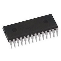
ATMEGA168PA-PU Atmel, ATMEGA168PA-PU Datasheet - Page 218

ATMEGA168PA-PU
Manufacturer Part Number
ATMEGA168PA-PU
Description
MCU, 8BIT, AVR, 16K FLASH, 28PDIP
Manufacturer
Atmel
Datasheet
1.ATMEGA48A-PU.pdf
(566 pages)
Specifications of ATMEGA168PA-PU
Controller Family/series
Atmega
No. Of I/o's
23
Eeprom Memory Size
512Byte
Ram Memory Size
1KB
Cpu Speed
20MHz
No.
RoHS Compliant
Core Size
8bit
Program Memory Size
16KB
Oscillator Type
External, Internal
Rohs Compliant
Yes
Available stocks
Company
Part Number
Manufacturer
Quantity
Price
Company:
Part Number:
ATMEGA168PA-PU
Manufacturer:
TI
Quantity:
1 240
- Current page: 218 of 566
- Download datasheet (23Mb)
21.3.3
21.3.4
8271C–AVR–08/10
Address Packet Format
Data Packet Format
All address packets transmitted on the TWI bus are 9 bits long, consisting of 7 address bits, one
READ/WRITE control bit and an acknowledge bit. If the READ/WRITE bit is set, a read opera-
tion is to be performed, otherwise a write operation should be performed. When a Slave
recognizes that it is being addressed, it should acknowledge by pulling SDA low in the ninth SCL
(ACK) cycle. If the addressed Slave is busy, or for some other reason can not service the Mas-
ter’s request, the SDA line should be left high in the ACK clock cycle. The Master can then
transmit a STOP condition, or a REPEATED START condition to initiate a new transmission. An
address packet consisting of a slave address and a READ or a WRITE bit is called SLA+R or
SLA+W, respectively.
The MSB of the address byte is transmitted first. Slave addresses can freely be allocated by the
designer, but the address 0000 000 is reserved for a general call.
When a general call is issued, all slaves should respond by pulling the SDA line low in the ACK
cycle. A general call is used when a Master wishes to transmit the same message to several
slaves in the system. When the general call address followed by a Write bit is transmitted on the
bus, all slaves set up to acknowledge the general call will pull the SDA line low in the ack cycle.
The following data packets will then be received by all the slaves that acknowledged the general
call. Note that transmitting the general call address followed by a Read bit is meaningless, as
this would cause contention if several slaves started transmitting different data.
All addresses of the format 1111 xxx should be reserved for future purposes.
Figure 21-4. Address Packet Format
All data packets transmitted on the TWI bus are nine bits long, consisting of one data byte and
an acknowledge bit. During a data transfer, the Master generates the clock and the START and
STOP conditions, while the Receiver is responsible for acknowledging the reception. An
Acknowledge (ACK) is signalled by the Receiver pulling the SDA line low during the ninth SCL
cycle. If the Receiver leaves the SDA line high, a NACK is signalled. When the Receiver has
received the last byte, or for some reason cannot receive any more bytes, it should inform the
Transmitter by sending a NACK after the final byte. The MSB of the data byte is transmitted first.
ATmega48A/48PA/88A/88PA/168A/168PA/328/328
SDA
SCL
START
Addr MSB
1
2
Addr LSB
7
R/W
8
ACK
9
218
Related parts for ATMEGA168PA-PU
Image
Part Number
Description
Manufacturer
Datasheet
Request
R

Part Number:
Description:
Manufacturer:
Atmel Corporation
Datasheet:

Part Number:
Description:
Manufacturer:
Atmel Corporation
Datasheet:

Part Number:
Description:
Manufacturer:
ATMEL Corporation
Datasheet:

Part Number:
Description:
IC AVR MCU 16K 20MHZ 32TQFP
Manufacturer:
Atmel
Datasheet:

Part Number:
Description:
IC AVR MCU 16K 20MHZ 32-QFN
Manufacturer:
Atmel
Datasheet:

Part Number:
Description:
IC AVR MCU 16K 20MHZ 28DIP
Manufacturer:
Atmel
Datasheet:

Part Number:
Description:
MCU AVR 16K FLASH 15MHZ 32-TQFP
Manufacturer:
Atmel
Datasheet:

Part Number:
Description:
MCU AVR 16K FLASH 15MHZ 32-QFN
Manufacturer:
Atmel
Datasheet:

Part Number:
Description:
IC AVR MCU 16K 20MHZ 32TQFP
Manufacturer:
Atmel
Datasheet:

Part Number:
Description:
MCU AVR 16KB FLASH 20MHZ 32QFN
Manufacturer:
Atmel
Datasheet:

Part Number:
Description:
MCU AVR 16KB FLASH 20MHZ 32TQFP
Manufacturer:
Atmel
Datasheet:

Part Number:
Description:
IC MCU AVR 16K FLASH 32-QFN
Manufacturer:
Atmel
Datasheet:


