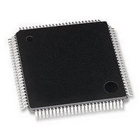
MB95F126JBPFR-GE1 Fujitsu, MB95F126JBPFR-GE1 Datasheet - Page 17

MB95F126JBPFR-GE1
Manufacturer Part Number
MB95F126JBPFR-GE1
Description
MCU, 8-BIT, 8FX, 32K FLASH, QFP100
Manufacturer
Fujitsu
Datasheet
1.MB95F126JBPF-GE1.pdf
(80 pages)
Specifications of MB95F126JBPFR-GE1
Controller Family/series
F2MC-8FX
No. Of I/o's
87
Ram Memory Size
1KB
Cpu Speed
16.25MHz
No. Of Timers
7
No. Of Pwm
RoHS Compliant
Core Size
8bit
Program Memory Size
32KB
Oscillator Type
External Only
DS07-12610-5E
■ HANDLING DEVICES
• Preventing Latch-up
• Stable Supply Voltage
• Precautions for Use of External Clock
• Serial communication
PIN CONNECTION
• Treatment of Unused Pin
• Treatment of Power Supply Pins on A/D Converter
Care must be taken to ensure that maximum voltage ratings are not exceeded when they are used.
Latch-up may occur on CMOS ICs if voltage higher than V
other than medium- and high-withstand voltage pins or if higher than the rating voltage is applied between V
pin and V
When latch-up occurs, power supply current increases rapidly and might thermally damage elements.
Also, take care to prevent the analog power supply voltage (AV
the digital power supply voltage (V
For stabilization, in principle, keep the variation in V
variation rate does not exceed 0.1 V/ms during a momentary change such as when the power supply is switched.
Even when an external clock is used, oscillation stabilization wait time is required for power-on reset, wake-up
from sub clock mode or stop mode.
There is a possibility to receive wrong data due to noise or other causes on the serial communication.
Therefore, design a printed circuit board so as to avoid noise.
Consider receiving of wrong data when designing the system. For example apply a checksum and retransmit
the data if an error occurs.
Leaving unused input pins unconnected can cause abnormal operation or latch-up, leaving to permanent
damage.
Unused input pins should always be pulled up or down through resistance of at least 2 kΩ. Any unused input/
output pins may be set to output mode and left open, or set to input mode and treated the same as unused input
pins. If there is unused output pin, make it open.
Connect to be AV
Noise riding on the AV
as a bypass capacitor between AV
Supply voltage should be stabilized.
A sudden change in power-supply voltage may cause a malfunction even within the guaranteed operating range
of the V
(50/60 Hz) not to exceed 10% of the standard V
CC
SS
power-supply voltage.
pin.
CC
= V
CC
CC
pin may cause accuracy degradation. So, connect approx. 0.1 μF ceramic capacitor
and AV
SS
CC
CC
= AVR = V
) when the analog system power supply is turned on or off.
and AV
SS
SS
pins in the vicinity of this device.
CC
even if the A/D converter is not in use.
value and suppress the voltage variation so that the transient
CC
ripple (p-p value) in a commercial frequency range
CC
or lower than V
CC
, AVR) and analog input voltage from exceeding
MB95120MB Series
SS
is applied to input and output pins
17
CC


