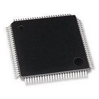
MB95F126JBPFR-GE1 Fujitsu, MB95F126JBPFR-GE1 Datasheet - Page 35

MB95F126JBPFR-GE1
Manufacturer Part Number
MB95F126JBPFR-GE1
Description
MCU, 8-BIT, 8FX, 32K FLASH, QFP100
Manufacturer
Fujitsu
Datasheet
1.MB95F126JBPF-GE1.pdf
(80 pages)
Specifications of MB95F126JBPFR-GE1
Controller Family/series
F2MC-8FX
No. Of I/o's
87
Ram Memory Size
1KB
Cpu Speed
16.25MHz
No. Of Timers
7
No. Of Pwm
RoHS Compliant
Core Size
8bit
Program Memory Size
32KB
Oscillator Type
External Only
DS07-12610-5E
(Continued)
*1 : The parameter is based on AV
*2 : Apply equal potential to AVcc and Vcc. AVR should not exceed AVcc + 0.3 V.
*3 : V0 to V3 should not exceed V
*4 : V
*5 : Applicable to pins : P00 to P07, P10 to P14, P20 to P24, P30 to P37, P40 to P43, P52, P53
WARNING: Semiconductor devices can be permanently damaged by application of stress (voltage, current,
Power consumption
Operating temperature
Storage temperature
• Input/Output Equivalent circuits
to/from an input is limited by some means with external components, the I
• Use within recommended operating conditions.
• Use at DC voltage (current).
• +B signal is an input signal that exceeds V
• The value of the limiting resistance should be set so that when the + B signal is applied the input current
• Note that when the microcontroller drive current is low, such as in the power saving modes, the +B input
• Note that if the + B signal is inputted when the microcontroller power supply is off (not fixed at 0 V), the power
• Note that if the + B input is applied during power-on, the power supply is provided from the pins and the
• Care must be taken not to leave the + B input pin open.
• Note that analog system input/output pins other than the A/D input pins (LCD drive pins, etc.) cannot accept
• Sample recommended circuits :
I
and Vo should not exceed V
resistance placed between the + B signal and the microcontroller.
to the microcontroller pin does not exceed rated values, either instantaneously or for prolonged periods.
potential may pass through the protective diode and increase the potential at the V
other devices.
supply is provided from the pins, so that incomplete operation may result.
resulting power supply voltage may not be sufficient to operate the power-on reset.
+B signal input.
Parameter
temperature, etc.) in excess of absolute maximum ratings. Do not exceed these ratings.
+ B input (0 V to 16 V)
Symbol
Tstg
Pd
T
A
CC
CC
SS
+ 0.3 V. V
+ 0.3 V.
= V
SS
resistance
Min
= 0.0 V.
− 40
− 55
⎯
I
Limiting
must not exceed the rating voltage. However, if the maximum current
Rating
CC
voltage. The + B signal should always be applied a limiting
+ 105
+ 150
Max
320
Protective diode
Unit
mW
°C
°C
MB95120MB Series
R
Vcc
CLAMP
P-ch
N-ch
rating supersedes the V
Remarks
CC
pin, and this affects
I
rating.
35


