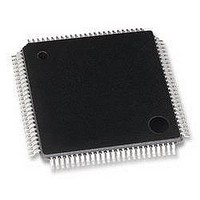
MB95F126JBPFR-GE1 Fujitsu, MB95F126JBPFR-GE1 Datasheet - Page 37

MB95F126JBPFR-GE1
Manufacturer Part Number
MB95F126JBPFR-GE1
Description
MCU, 8-BIT, 8FX, 32K FLASH, QFP100
Manufacturer
Fujitsu
Datasheet
1.MB95F126JBPF-GE1.pdf
(80 pages)
Specifications of MB95F126JBPFR-GE1
Controller Family/series
F2MC-8FX
No. Of I/o's
87
Ram Memory Size
1KB
Cpu Speed
16.25MHz
No. Of Timers
7
No. Of Pwm
RoHS Compliant
Core Size
8bit
Program Memory Size
32KB
Oscillator Type
External Only
- Current page: 37 of 80
- Download datasheet (3Mb)
DS07-12610-5E
3. DC Characteristics
“H” level input
voltage
“L” level input
voltage
Parameter
Symbol
V
V
V
V
V
V
V
V
IHS1
IHS2
IHA
IHM
IH1
IH2
ILA
IL
P10 (selectable at UI0) ,
P67 (selectable at SIN)
P50, P51
P00 to P07, P10 to P14,
P20 to P24, P30 to P37,
P40 to P43, P50 to P53,
P60 to P67, P70, P71,
P90 to P95,
PA0 to PA3,
PB0 to PB7,
PC0 to PC7,
PD0 to PD7,
PE0 to PE7
P00 to P07, P10 to P14,
P20 to P24, P30 to P37,
P40 to P43, P50 to P53,
P60 to P67, P70, P71,
P90 to P95,
PA0 to PA3,
PB0 to PB7,
PC0 to PC7,
PD0 to PD7,
PE0 to PE7
P50, P51
RST, MOD
P10 (selectable at UI0) ,
P50, P51
P67 (selectable at SIN)
P00 to P07, P10 to P14,
P20 to P24, P30 to P37,
P40 to P43, P50 to P53,
P60 to P67, P70, P71,
P90 to P95,
PA0 to PA3,
PB0 to PB7,
PC0 to PC7,
PD0 to PD7,
PE0 to PE7
(selectable at I
(selectable at I
Pin name
(V
CC
2
2
C)
C)
= AV
CC
= 5.0 V ± 10%, AV
Condi-
tion
⎯
⎯
⎯
⎯
⎯
⎯
⎯
⎯
⎯
V
V
0.7 V
0.7 V
0.8 V
0.8 V
0.8 V
0.7 V
0.8 V
SS
SS
Min
− 0.3
− 0.3
CC
CC
CC
CC
CC
CC
CC
MB95120MB Series
SS
Value
Typ
⎯
⎯
⎯
⎯
⎯
⎯
⎯
⎯
⎯
= V
SS
V
V
V
V
V
V
V
0.3 V
0.5 V
= 0.0 V, T
CC
SS
CC
CC
SS
CC
CC
Max
+ 5.5
+ 5.5
+ 0.3
+ 0.3
+ 0.3
+ 0.3
+ 0.3
CC
CC
Unit
A
V
V
V
V
V
V
V
V
V
= − 40 °C to + 105 °C)
Hysteresis input
CMOS input level)
Port inputs if Auto-
motive input levels
are selected
Hysteresis input
CMOS input
product)
Hysteresis input
(MASK ROM
product)
Hysteresis input
CMOS input level)
Port inputs if
Automotive input
levels are selected
(When selecting
(Flash memory
(When selecting
Remarks
(Continued)
37
Related parts for MB95F126JBPFR-GE1
Image
Part Number
Description
Manufacturer
Datasheet
Request
R

Part Number:
Description:
Fujitsu Media Devices Limited [NMOS 1- CHANNEL, 13-BIT AND 3-CHANNEL, 6-BIT D/A CONVERTER]
Manufacturer:
Fujitsu
Datasheet:

Part Number:
Description:
Fujitsu Media Devices Limited [32-bit RISC Microcontroller]
Manufacturer:
Fujitsu
Datasheet:

Part Number:
Description:
Fujitsu Media Devices Limited [MOS 262,144 BIT DYNAMIC RANDOM ACCESS MEMORY]
Manufacturer:
Fujitsu
Datasheet:

Part Number:
Description:
Fujitsu Media Devices Limited [PROGRAMMABLE TIMER]
Manufacturer:
Fujitsu
Datasheet:

Part Number:
Description:
Fujitsu Media Devices Limited [MOS Universal Asynchronous receiver/transmitter(UART)]
Manufacturer:
Fujitsu
Datasheet:

Part Number:
Description:
Fujitsu Media Devices Limited [16M (2M X 8/1M X 16) BIT]
Manufacturer:
Fujitsu
Datasheet:

Part Number:
Description:
KIT, STARTER, MB95200/210/220
Manufacturer:
Fujitsu
Datasheet:

Part Number:
Description:
SWITCHING REGULATOR CONTROLLER
Manufacturer:
Fujitsu
Datasheet:

Part Number:
Description:
QUAD OPERATIONAL AMPLIFIER
Manufacturer:
Fujitsu
Datasheet:

Part Number:
Description:
Switching Regulator Controller (Switchable between push-pull and single-end functions)
Manufacturer:
Fujitsu
Datasheet:

Part Number:
Description:
HIGH-SPEED CMOS SINGLE CHIP 4-BIT MICROCOMPUTER MB88505HHIGH-SPEED CMOS SINGLE CHIP 4-BIT MICROCOMPUTER
Manufacturer:
Fujitsu
Datasheet:

Part Number:
Description:
MOS 1024 BIT NON VOLATILE RANDOM ACCESS MEMORY
Manufacturer:
Fujitsu
Datasheet:

Part Number:
Description:
Schottky TTL 2048-Bit Bipolar Programmable Read-Only Memory
Manufacturer:
Fujitsu
Datasheet:

Part Number:
Description:
QUAD COMPARATOR
Manufacturer:
Fujitsu
Datasheet:


