IPR-QDRII/UNI Altera, IPR-QDRII/UNI Datasheet - Page 31
IPR-QDRII/UNI
Manufacturer Part Number
IPR-QDRII/UNI
Description
IP CORE Renewal Of IP-QDRII/UNI
Manufacturer
Altera
Datasheet
1.IP-QDRIIUNI.pdf
(74 pages)
Specifications of IPR-QDRII/UNI
Software Application
IP CORE, Memory Controllers, SRAM
Supported Families
Arria II GX, HardCopy III, Stratix III, Stratix IV
Core Architecture
FPGA
Core Sub-architecture
Arria, HardCopy, Stratix
Rohs Compliant
NA
Lead Free Status / RoHS Status
na


Chapter 3: Parameter Settings
Memory Timing
Memory Timing
December 2010 Altera Corporation
Table 3–5. Memory Parameters (Part 2 of 2)
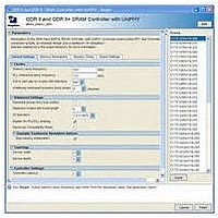
The Memory Timing tab allows you to configure memory device timing parameters.
You can enter timing parameters manually from the manufacturer’s device data sheet,
or you can populate the fields automatically by selecting the required device from the
list of presets.
Table 3–6
Table 3–6. Memory Timing Parameters
Data-mask width
CQ width
K width
Burst length
tWL (cycles)
tRL (cycles)
tSA
tHA
tSD
tHD
tCQD
tCQDOH
Internal jitter
TCQHCQnH
TKHKnH
describes the memory timing parameters.
Parameters
Parameter
Section III. QDR II and QDR II+ SRAM Controller with UniPHY User Guide
The width of the data-mask on the memory device,
The width of the CQ (read strobe) bus on the memory
device.
The width of the K (write strobe) bus on the memory
device.
The burst length supported by the memory device.
The write latency.
The read latency.
The address and control setup to K clock rise.
The address and control hold after K clock rise.
The data setup to clock (K/K#) rise.
The data hold after clock (K/K#) rise.
Echo clock high to data valid.
Echo clock high to data invalid.
The QDRII/II+ internal jitter.
The CQ clock rise to CQn clock rise (rising edge to rising
edge).
The K clock rise to Kn clock rise (rising edge to rising
edge).
External Memory Interface Handbook Volume 3
Description
Description
3–3
Related parts for IPR-QDRII/UNI
Image
Part Number
Description
Manufacturer
Datasheet
Request
R

Part Number:
Description:
CYCLONE II STARTER KIT EP2C20N
Manufacturer:
Altera
Datasheet:


Part Number:
Description:
CPLD, EP610 Family, ECMOS Process, 300 Gates, 16 Macro Cells, 16 Reg., 16 User I/Os, 5V Supply, 35 Speed Grade, 24DIP
Manufacturer:
Altera Corporation
Datasheet:
Part Number:
Description:
CPLD, EP610 Family, ECMOS Process, 300 Gates, 16 Macro Cells, 16 Reg., 16 User I/Os, 5V Supply, 15 Speed Grade, 24DIP
Manufacturer:
Altera Corporation
Datasheet:
Part Number:
Description:
Manufacturer:
Altera Corporation
Datasheet:
Part Number:
Description:
CPLD, EP610 Family, ECMOS Process, 300 Gates, 16 Macro Cells, 16 Reg., 16 User I/Os, 5V Supply, 30 Speed Grade, 24DIP
Manufacturer:
Altera Corporation
Datasheet:
Part Number:
Description:
High-performance, low-power erasable programmable logic devices with 8 macrocells, 10ns
Manufacturer:
Altera Corporation
Datasheet:
Part Number:
Description:
High-performance, low-power erasable programmable logic devices with 8 macrocells, 7ns
Manufacturer:
Altera Corporation
Datasheet:
Part Number:
Description:
Classic EPLD
Manufacturer:
Altera Corporation
Datasheet:
Part Number:
Description:
High-performance, low-power erasable programmable logic devices with 8 macrocells, 10ns
Manufacturer:
Altera Corporation
Datasheet:
Part Number:
Description:
Manufacturer:
Altera Corporation
Datasheet:
Part Number:
Description:
Manufacturer:
Altera Corporation
Datasheet:
Part Number:
Description:
Manufacturer:
Altera Corporation
Datasheet:
Part Number:
Description:
CPLD, EP610 Family, ECMOS Process, 300 Gates, 16 Macro Cells, 16 Reg., 16 User I/Os, 5V Supply, 25 Speed Grade, 24DIP
Manufacturer:
Altera Corporation
Datasheet: