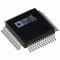
ADUC836BSZ Analog Devices Inc, ADUC836BSZ Datasheet - Page 12

ADUC836BSZ
Manufacturer Part Number
ADUC836BSZ
Description
16bit Dual ADC With Embedded 8 Bit MCU
Manufacturer
Analog Devices Inc
Series
MicroConverter® ADuC8xxr
Datasheet
1.ADUC836BSZ.pdf
(80 pages)
Specifications of ADUC836BSZ
Core Processor
8052
Core Size
8-Bit
Speed
12.58MHz
Connectivity
EBI/EMI, I²C, SPI, UART/USART
Peripherals
POR, PSM, PWM, Temp Sensor, WDT
Number Of I /o
34
Program Memory Size
62KB (62K x 8)
Program Memory Type
FLASH
Eeprom Size
4K x 8
Ram Size
2.25K x 8
Voltage - Supply (vcc/vdd)
2.7 V ~ 5.25 V
Data Converters
A/D 7x16b; D/A 1x12b
Oscillator Type
Internal
Operating Temperature
-40°C ~ 125°C
Package / Case
52-MQFP, 52-PQFP
Cpu Family
ADuC8xx
Device Core
8052
Device Core Size
8b
Frequency (max)
12.58MHz
Interface Type
I2C/SPI/UART
Total Internal Ram Size
2.25KB
# I/os (max)
26
Number Of Timers - General Purpose
3
Operating Supply Voltage (typ)
3.3/5V
Operating Supply Voltage (max)
5.25V
Operating Supply Voltage (min)
2.7V
On-chip Adc
2(2-chx16-bit)
On-chip Dac
1-chx12-bit
Instruction Set Architecture
CISC
Operating Temp Range
-40C to 125C
Operating Temperature Classification
Automotive
Mounting
Surface Mount
Pin Count
52
Package Type
MQFP
Package
52MQFP
Family Name
ADuC8xx
Maximum Speed
12.58 MHz
Operating Supply Voltage
3.3|5 V
Data Bus Width
8 Bit
Number Of Programmable I/os
26
Number Of Timers
3
Lead Free Status / RoHS Status
Lead free / RoHS Compliant
Lead Free Status / RoHS Status
Lead free / RoHS Compliant
Available stocks
Company
Part Number
Manufacturer
Quantity
Price
Company:
Part Number:
ADUC836BSZ
Manufacturer:
ADI
Quantity:
150
Company:
Part Number:
ADUC836BSZ
Manufacturer:
Analog Devices Inc
Quantity:
10 000
Part Number:
ADUC836BSZ
Manufacturer:
ADI/亚德诺
Quantity:
20 000
52-Lead 56-Lead
MQFP
40
41
42
43–46
49–52
*I = Input, O = Output, S = Supply.
ADuC836
Pin No. Pin No.
CSP
43
44
45
46–49
52–55
Mnemonic
EA
PSEN
ALE
P0.0–P0.7
(AD0–AD3)
Type* Description
I/O
O
O
I/O
PIN FUNCTION DESCRIPTIONS (continued)
External Access Enable, Logic Input. When held high, this input enables the device to
fetch code from internal program memory locations 0000h to F7FFh. When held low,
this input enables the device to fetch all instructions from external program memory.
To determine the mode of code execution, i.e., internal or external, the EA pin is
sampled at the end of an external RESET assertion or as part of a device power cycle.
EA may also be used as an external emulation I/O pin, and therefore the voltage level
at this pin must not be changed during normal mode operation as it may cause an
emulation interrupt that will halt code execution.
Program Store Enable, Logic Output. This output is a control signal that enables the
external program memory to the bus during external fetch operations. It is active every
six oscillator periods except during external data memory accesses. This pin remains
high during internal program execution. PSEN can also be used to enable Serial
Download mode when pulled low through a resistor at the end of an external RESET
assertion or as part of a device power cycle.
Address Latch Enable, Logic Output. This output is used to latch the low byte (and
page byte for 24-bit data address space accesses) of the address to external memory
during external code or data memory access cycles. It is activated every six oscillator
periods except during an external data memory access. It can be disabled by setting
the PCON.4 bit in the PCON SFR.
These pins are part of Port 0, which is an 8-bit, open-drain, bidirectional
I/O port. Port 0 pins that have 1s written to them float and in that state can be used
(AD4–AD7)as high impedance inputs. An external pull-up resistor will be required
on P0 outputs to force a valid logic high level externally. Port 0 is also the multiplexed
low order address and data bus during accesses to external program or data memory.
In this application, it uses strong internal pull-ups when emitting 1s.
–12–
REV. A


