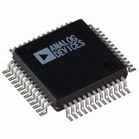
ADUC836BSZ Analog Devices Inc, ADUC836BSZ Datasheet - Page 14

ADUC836BSZ
Manufacturer Part Number
ADUC836BSZ
Description
16bit Dual ADC With Embedded 8 Bit MCU
Manufacturer
Analog Devices Inc
Series
MicroConverter® ADuC8xxr
Datasheet
1.ADUC836BSZ.pdf
(80 pages)
Specifications of ADUC836BSZ
Core Processor
8052
Core Size
8-Bit
Speed
12.58MHz
Connectivity
EBI/EMI, I²C, SPI, UART/USART
Peripherals
POR, PSM, PWM, Temp Sensor, WDT
Number Of I /o
34
Program Memory Size
62KB (62K x 8)
Program Memory Type
FLASH
Eeprom Size
4K x 8
Ram Size
2.25K x 8
Voltage - Supply (vcc/vdd)
2.7 V ~ 5.25 V
Data Converters
A/D 7x16b; D/A 1x12b
Oscillator Type
Internal
Operating Temperature
-40°C ~ 125°C
Package / Case
52-MQFP, 52-PQFP
Cpu Family
ADuC8xx
Device Core
8052
Device Core Size
8b
Frequency (max)
12.58MHz
Interface Type
I2C/SPI/UART
Total Internal Ram Size
2.25KB
# I/os (max)
26
Number Of Timers - General Purpose
3
Operating Supply Voltage (typ)
3.3/5V
Operating Supply Voltage (max)
5.25V
Operating Supply Voltage (min)
2.7V
On-chip Adc
2(2-chx16-bit)
On-chip Dac
1-chx12-bit
Instruction Set Architecture
CISC
Operating Temp Range
-40C to 125C
Operating Temperature Classification
Automotive
Mounting
Surface Mount
Pin Count
52
Package Type
MQFP
Package
52MQFP
Family Name
ADuC8xx
Maximum Speed
12.58 MHz
Operating Supply Voltage
3.3|5 V
Data Bus Width
8 Bit
Number Of Programmable I/os
26
Number Of Timers
3
Lead Free Status / RoHS Status
Lead free / RoHS Compliant
Lead Free Status / RoHS Status
Lead free / RoHS Compliant
Available stocks
Company
Part Number
Manufacturer
Quantity
Price
Company:
Part Number:
ADUC836BSZ
Manufacturer:
ADI
Quantity:
150
Company:
Part Number:
ADUC836BSZ
Manufacturer:
Analog Devices Inc
Quantity:
10 000
Part Number:
ADUC836BSZ
Manufacturer:
ADI/亚德诺
Quantity:
20 000
When accessing the internal XRAM, the P0 and P2 port pins, as
well as the RD and WR strobes, will not be output as per a stan-
dard 8051 MOVX instruction. This allows the user to use these
port pins as standard I/O.
The upper 1792 bytes of the internal XRAM can be configured
to be used as an extended 11-bit stack pointer. By default, the
stack will operate exactly like an 8052 in that it will roll over from
FFH to 00H in the general-purpose RAM. On the ADuC836
however, it is possible (by setting CFG836.7) to enable the 11-bit
extended stack pointer. In this case, the stack will roll over from
FFH in RAM to 0100H in XRAM. The 11-bit stack pointer is
visible in the SP and SPH SFRs. The SP SFR is located at 81H
as with a standard 8052. The SPH SFR is located at B7H. The
3 LSBs of this SFR contain the three extra bits necessary to
extend the 8-bit stack pointer into an 11-bit stack pointer.
External Data Memory (External XRAM)
Just like a standard 8051 compatible core, the ADuC836 can
access external data memory using a MOVX instruction. The
MOVX instruction automatically outputs the various control
strobes required to access the data memory.
The ADuC836, however, can access up to 16 Mbytes of external
data memory. This is an enhancement of the 64 Kbytes external
data memory space available on a standard 8051 compatible core.
The external data memory is discussed in more detail in the
ADuC836 Hardware Design Considerations section.
ADuC836
Figure 4. Extended Stack Pointer Operation
CFG836.7 = 0
FFH
00H
ON-CHIP DATA
256 BYTES OF
(DATA +
STACK)
RAM
CFG836.7 = 1
07FFH
100H
00H
(DATA + STACK
ON-CHIP XRAM
ON-CHIP XRAM
FOR EXSP = 1,
FOR EXSP = 0)
(DATA ONLY)
UPPER 1792
DATA ONLY
LOWER 256
BYTES OF
BYTES OF
–14–
SPECIAL FUNCTION REGISTERS (SFRS)
The SFR space is mapped into the upper 128 bytes of internal
data memory space and accessed by direct addressing only. It
provides an interface between the CPU and all on-chip periph-
erals. A block diagram showing the programming model of the
ADuC836 via the SFR area is shown in Figure 5.
All registers, except the Program Counter (PC) and the four
general-purpose register banks, reside in the SFR area. The SFR
registers include control, configuration, and data registers that
provide an interface between the CPU and all on-chip peripherals.
Accumulator SFR (ACC)
ACC is the Accumulator Register, which is used for math
operations including addition, subtraction, integer multiplication,
and division, and Boolean bit manipulations. The mnemonics for
accumulator-specific instructions, refer to the Accumulator as A.
B SFR (B)
The B Register is used with the ACC for multiplication and
division operations. For other instructions, it can be treated as a
general-purpose scratch pad register.
Data Pointer (DPTR)
The Data Pointer is made up of three 8-bit registers, named DPP
(page byte), DPH (high byte), and DPL (low byte). These are
used to provide memory addresses for internal and external code
access and external data access. It may be manipulated as a 16-bit
register (DPTR = DPH, DPL), although INC DPTR instructions
will automatically carry over to DPP, or as three independent 8-bit
registers (DPP, DPH, DPL).
The ADuC836 supports dual data pointers. For more information,
refer to the Dual Data Pointer section.
62 KBYTE ELECTRICALLY
NONVOLATILE FLASH/EE
REPROGRAMMABLE
PROGRAM MEMORY
256 BYTES RAM
COMPATIBLE
2K XRAM
CORE
8051
Figure 5. Programming Model
FUNCTION
REGISTER
128-BYTE
SPECIAL
AREA
REPROGRAMMABLE
CURRENT SOURCES
OTHER ON-CHIP
FLASH/EE DATA
ELECTRICALLY
DUAL - ADCs
TEMP SENSOR
NONVOLATILE
PERIPHERALS
12-BIT DAC
SERIAL I/O
WDT, PSM
MEMORY
4 KBYTE
TIC, PLL
REV. A


