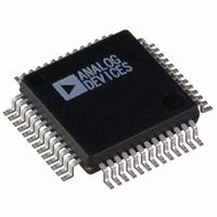
ADUC836BSZ Analog Devices Inc, ADUC836BSZ Datasheet - Page 78

ADUC836BSZ
Manufacturer Part Number
ADUC836BSZ
Description
16bit Dual ADC With Embedded 8 Bit MCU
Manufacturer
Analog Devices Inc
Series
MicroConverter® ADuC8xxr
Datasheet
1.ADUC836BSZ.pdf
(80 pages)
Specifications of ADUC836BSZ
Core Processor
8052
Core Size
8-Bit
Speed
12.58MHz
Connectivity
EBI/EMI, I²C, SPI, UART/USART
Peripherals
POR, PSM, PWM, Temp Sensor, WDT
Number Of I /o
34
Program Memory Size
62KB (62K x 8)
Program Memory Type
FLASH
Eeprom Size
4K x 8
Ram Size
2.25K x 8
Voltage - Supply (vcc/vdd)
2.7 V ~ 5.25 V
Data Converters
A/D 7x16b; D/A 1x12b
Oscillator Type
Internal
Operating Temperature
-40°C ~ 125°C
Package / Case
52-MQFP, 52-PQFP
Cpu Family
ADuC8xx
Device Core
8052
Device Core Size
8b
Frequency (max)
12.58MHz
Interface Type
I2C/SPI/UART
Total Internal Ram Size
2.25KB
# I/os (max)
26
Number Of Timers - General Purpose
3
Operating Supply Voltage (typ)
3.3/5V
Operating Supply Voltage (max)
5.25V
Operating Supply Voltage (min)
2.7V
On-chip Adc
2(2-chx16-bit)
On-chip Dac
1-chx12-bit
Instruction Set Architecture
CISC
Operating Temp Range
-40C to 125C
Operating Temperature Classification
Automotive
Mounting
Surface Mount
Pin Count
52
Package Type
MQFP
Package
52MQFP
Family Name
ADuC8xx
Maximum Speed
12.58 MHz
Operating Supply Voltage
3.3|5 V
Data Bus Width
8 Bit
Number Of Programmable I/os
26
Number Of Timers
3
Lead Free Status / RoHS Status
Lead free / RoHS Compliant
Lead Free Status / RoHS Status
Lead free / RoHS Compliant
Available stocks
Company
Part Number
Manufacturer
Quantity
Price
Company:
Part Number:
ADUC836BSZ
Manufacturer:
ADI
Quantity:
150
Company:
Part Number:
ADUC836BSZ
Manufacturer:
Analog Devices Inc
Quantity:
10 000
Part Number:
ADUC836BSZ
Manufacturer:
ADI/亚德诺
Quantity:
20 000
Parameter
SPI SLAVE MODE TIMING (CPHA = 0)
ADuC836
t
t
t
t
t
t
t
t
t
t
t
t
t
SS
SL
SH
DAV
DSU
DHD
DF
DR
SR
SF
SSR
DOSS
SFS
(CPOL = 0)
(CPOL = 1)
SCLOCK
SCLOCK
SS to SCLOCK Edge
SCLOCK Low Pulsewidth
SCLOCK High Pulsewidth
Data Output Valid after SCLOCK Edge
Data Input Setup Time before SCLOCK Edge
Data Input Hold Time after SCLOCK Edge
Data Output Fall Time
Data Output Rise Time
SCLOCK Rise Time
SCLOCK Fall Time
SS to SCLOCK Edge
Data Output Valid after SS Edge
SS High after SCLOCK Edge
MISO
MOSI
SS
t
DOSS
t
SS
t
DSU
MSB IN
Figure 78. SPI Slave ModeTiming (CPHA = 0)
MSB
t
DHD
t
SH
t
DF
t
DAV
t
SL
t
DR
BITS 6–1
BITS 6–1
–78–
Min
0
100
100
0
Typ
330
330
10
10
10
10
LSB IN
t
SR
LSB
Max
50
25
25
25
25
50
20
t
SF
t
SFS
Unit
ns
ns
ns
ns
ns
ns
ns
ns
ns
ns
ns
ns
ns
REV. A


