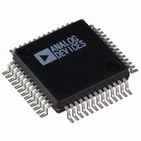
ADUC836BSZ Analog Devices Inc, ADUC836BSZ Datasheet - Page 35

ADUC836BSZ
Manufacturer Part Number
ADUC836BSZ
Description
16bit Dual ADC With Embedded 8 Bit MCU
Manufacturer
Analog Devices Inc
Series
MicroConverter® ADuC8xxr
Datasheet
1.ADUC836BSZ.pdf
(80 pages)
Specifications of ADUC836BSZ
Core Processor
8052
Core Size
8-Bit
Speed
12.58MHz
Connectivity
EBI/EMI, I²C, SPI, UART/USART
Peripherals
POR, PSM, PWM, Temp Sensor, WDT
Number Of I /o
34
Program Memory Size
62KB (62K x 8)
Program Memory Type
FLASH
Eeprom Size
4K x 8
Ram Size
2.25K x 8
Voltage - Supply (vcc/vdd)
2.7 V ~ 5.25 V
Data Converters
A/D 7x16b; D/A 1x12b
Oscillator Type
Internal
Operating Temperature
-40°C ~ 125°C
Package / Case
52-MQFP, 52-PQFP
Cpu Family
ADuC8xx
Device Core
8052
Device Core Size
8b
Frequency (max)
12.58MHz
Interface Type
I2C/SPI/UART
Total Internal Ram Size
2.25KB
# I/os (max)
26
Number Of Timers - General Purpose
3
Operating Supply Voltage (typ)
3.3/5V
Operating Supply Voltage (max)
5.25V
Operating Supply Voltage (min)
2.7V
On-chip Adc
2(2-chx16-bit)
On-chip Dac
1-chx12-bit
Instruction Set Architecture
CISC
Operating Temp Range
-40C to 125C
Operating Temperature Classification
Automotive
Mounting
Surface Mount
Pin Count
52
Package Type
MQFP
Package
52MQFP
Family Name
ADuC8xx
Maximum Speed
12.58 MHz
Operating Supply Voltage
3.3|5 V
Data Bus Width
8 Bit
Number Of Programmable I/os
26
Number Of Timers
3
Lead Free Status / RoHS Status
Lead free / RoHS Compliant
Lead Free Status / RoHS Status
Lead free / RoHS Compliant
Available stocks
Company
Part Number
Manufacturer
Quantity
Price
Company:
Part Number:
ADUC836BSZ
Manufacturer:
ADI
Quantity:
150
Company:
Part Number:
ADUC836BSZ
Manufacturer:
Analog Devices Inc
Quantity:
10 000
Part Number:
ADUC836BSZ
Manufacturer:
ADI/亚德诺
Quantity:
20 000
Note that Figure 22 represents a transfer function in 0-to-V
only. In 0-to-V
would be similar, but the upper portion of the transfer function
would follow the “ideal” line right to the end, showing no signs of
endpoint linearity errors.
The endpoint nonlinearities conceptually illustrated in Figure 22
get worse as a function of output loading. Most of the ADuC836
data sheet specifications assume a 10 k resistive load to ground
at the DAC output. As the output is forced to source or sink more
current, the nonlinear regions at the top or bottom (respectively)
of Figure 22 become larger. With larger current demands, this
can significantly limit output voltage swing. Figures 23 and 24
illustrate this behavior. It should be noted that the upper trace in
each of these figures is valid only for an output range selection of
0-to-AV
side voltage drops as long as the reference voltage remains below
the upper trace in the corresponding figure. For example, if AV
= 3 V and V
loads less than 5 mA. But somewhere around 7 mA, the upper curve
in Figure 24 drops below 2.5 V (V
higher currents, the output will not be capable of reaching V
REV. A
V
V
DD
DD
–100mV
–50mV
100mV
50mV
Figure 23. Source and Sink Current Capability
with V
0mV
V
DD
Figure 22. Endpoint Nonlinearities Due to
Amplifier Saturation
DD
4
5
3
2
1
0
. In 0-to-V
0
REF
000H
REF
REF
= 2.5 V, the high side voltage will not be affected by
= AV
mode (with V
REF
DD
SOURCE/SINK CURRENT – mA
= 5 V
mode, DAC loading will not cause high
5
DAC LOADED WITH 0FFFH
DAC LOADED WITH 0000H
REF
REF
< V
), indicating that at these
DD
), the lower nonlinearity
10
DD
15
FFFH
mode
REF
DD
.
–35–
For larger loads, the current drive capability may not be sufficient
To increase the source and sink current capability of the DAC, an
external buffer should be added, as shown in Figure 25.
The DAC output buffer also features a high impedance disable func-
tion. In the chip’s default power-on state, the DAC is disabled and
its output is in a high impedance state (or “three-state”) where
they remain inactive until enabled in software.
This means that if a zero output is desired during power-up or
power-down transient conditions, a pull-down resistor must be
added to each DAC output. Assuming this resistor is in place, the
DAC output will remain at ground potential whenever the DAC
is disabled.
Figure 24. Source and Sink Current Capability with
V
REF
4
3
1
0
0
= V
Figure 25. Buffering the DAC Output
ADuC836
DD
DAC LOADED WITH 0FFFH
DAC LOADED WITH 0000H
= 3 V
SOURCE/SINK CURRENT – mA
12
5
10
ADuC836
15


