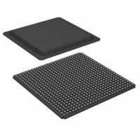
XC3SD3400A-4FGG676C Xilinx Inc, XC3SD3400A-4FGG676C Datasheet - Page 44

XC3SD3400A-4FGG676C
Manufacturer Part Number
XC3SD3400A-4FGG676C
Description
FPGA, SPARTAN-3A, DSP, 676FBGA
Manufacturer
Xilinx Inc
Series
Spartan™-3A DSPr
Datasheets
1.XC3S50A-4VQG100C.pdf
(7 pages)
2.XC3SD3400A-4FGG676C.pdf
(4 pages)
3.XC3SD3400A-4FGG676C.pdf
(101 pages)
Specifications of XC3SD3400A-4FGG676C
No. Of Logic Blocks
5968
No. Of Gates
3400000
No. Of Macrocells
53712
Family Type
Spartan-3A
No. Of Speed Grades
4
Total Ram Bits
2322432
No. Of I/o's
502
Clock Management
DCM
I/o Supply
RoHS Compliant
Number Of Logic Elements/cells
53712
Number Of Labs/clbs
5968
Number Of I /o
469
Number Of Gates
3400000
Voltage - Supply
1.14 V ~ 1.26 V
Mounting Type
Surface Mount
Operating Temperature
0°C ~ 85°C
Package / Case
676-BBGA
Package
676FBGA
Family Name
Spartan®-3A
Device Logic Units
53712
Device System Gates
3400000
Maximum Internal Frequency
667 MHz
Typical Operating Supply Voltage
1.2 V
Maximum Number Of User I/os
469
Ram Bits
2322432
Rohs Compliant
Yes
Lead Free Status / RoHS Status
Lead free / RoHS Compliant
For Use With
122-1532 - KIT DEVELOPMENT SPARTAN 3ADSP
Lead Free Status / RoHS Status
Lead free / RoHS Compliant
Other names
122-1539
Available stocks
Company
Part Number
Manufacturer
Quantity
Price
Company:
Part Number:
XC3SD3400A-4FGG676C
Manufacturer:
XilinxInc
Quantity:
3 000
Company:
Part Number:
XC3SD3400A-4FGG676C
Manufacturer:
Xilinx Inc
Quantity:
10 000
Company:
Part Number:
XC3SD3400A-4FGG676C
Manufacturer:
XILINX
Quantity:
592
Part Number:
XC3SD3400A-4FGG676C
Manufacturer:
XILINX/赛灵思
Quantity:
20 000
Digital Clock Manager (DCM) Timing
For specification purposes, the DCM consists of three key
components: the Delay-Locked Loop (DLL), the Digital
Frequency Synthesizer (DFS), and the Phase Shifter (PS).
Aspects of DLL operation play a role in all DCM
applications. All such applications inevitably use the CLKIN
and the CLKFB inputs connected to either the CLK0 or the
CLK2X feedback, respectively. Thus, specifications in the
DLL tables
that only employs the DLL component. When the DFS
and/or the PS components are used together with the DLL,
then the specifications listed in the DFS and PS tables
(Table 38
ones in the DLL tables. DLL specifications that do not
change with the addition of DFS or PS functions are
presented in
Period jitter and cycle-cycle jitter are two of many different
ways of specifying clock jitter. Both specifications describe
statistical variation from a mean value.
Delay-Locked Loop (DLL)
Table 36: Recommended Operating Conditions for the DLL
DS610 (v3.0) October 4, 2010
Product Specification
Notes:
1.
2.
3.
4.
5.
Input Frequency Ranges
F
Input Pulse Requirements
CLKIN_PULSE
Input Clock Jitter Tolerance and Delay Path Variation
CLKIN_CYC_JITT_DLL_LF
CLKIN_CYC_JITT_DLL_HF
CLKIN_PER_JITT_DLL
CLKFB_DELAY_VAR_EXT
CLKIN
DLL specifications apply when any of the DLL outputs (CLK0, CLK90, CLK180, CLK270, CLK2X, CLK2X180, or CLKDV) are in use.
The DFS, when operating independently of the DLL, supports lower FCLKIN frequencies. See
To support double the maximum effective FCLKIN limit, set the CLKIN_DIVIDE_BY_2 attribute to TRUE. This attribute divides the incoming
clock frequency by two as it enters the DCM. The CLK2X output reproduces the clock frequency provided on the CLKIN input.
CLKIN input jitter beyond these limits might cause the DCM to lose lock.
The DCM specifications are guaranteed when both adjacent DCMs are locked.
through
CLKIN_FREQ_DLL
(Table 36
Symbol
Table 36
Table
and
and
41) supersede any corresponding
Table
Table
37) apply to any application
37.
Allowable variation of off-chip feedback delay
Frequency of the CLKIN clock input
CLKIN pulse width as a
percentage of the CLKIN
period
Cycle-to-cycle jitter at the
CLKIN input
Period jitter at the CLKIN input
from the DCM output to the CLKFB input
Description
Spartan-3A DSP FPGA Family: DC and Switching Characteristics
(4)
www.xilinx.com
F
F
F
F
CLKIN
CLKIN
CLKIN
CLKIN
Period jitter is the worst-case deviation from the ideal clock
period over a collection of millions of samples. In a
histogram of period jitter, the mean value is the clock period.
Cycle-cycle jitter is the worst-case difference in clock period
between adjacent clock cycles in the collection of clock
periods sampled. In a histogram of cycle-cycle jitter, the
mean value is zero.
Spread Spectrum
DCMs accept typical spread spectrum clocks as long as
they meet the input requirements. The DLL will track the
frequency changes created by the spread spectrum clock to
drive the global clocks to the FPGA logic. See XAPP469:
Spread-Spectrum Clocking Reception for Displays for
details.
< 150 MHz
> 150 MHz
< 150 MHz
> 150 MHz
40%
45%
Min
5
–
–
–
–
(2)
Table
-5
280
±300
±150
Speed Grade
Max
60%
55%
38.
±1
±1
(3)
40%
45%
Min
5
–
–
–
–
(2)
-4
250
±300
±150
Max
60%
55%
±1
±1
(3)
Units
MHz
ps
ps
ns
ns
–
–
44


