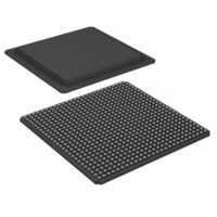
XC3SD3400A-4FGG676C Xilinx Inc, XC3SD3400A-4FGG676C Datasheet - Page 59

XC3SD3400A-4FGG676C
Manufacturer Part Number
XC3SD3400A-4FGG676C
Description
FPGA, SPARTAN-3A, DSP, 676FBGA
Manufacturer
Xilinx Inc
Series
Spartan™-3A DSPr
Datasheets
1.XC3S50A-4VQG100C.pdf
(7 pages)
2.XC3SD3400A-4FGG676C.pdf
(4 pages)
3.XC3SD3400A-4FGG676C.pdf
(101 pages)
Specifications of XC3SD3400A-4FGG676C
No. Of Logic Blocks
5968
No. Of Gates
3400000
No. Of Macrocells
53712
Family Type
Spartan-3A
No. Of Speed Grades
4
Total Ram Bits
2322432
No. Of I/o's
502
Clock Management
DCM
I/o Supply
RoHS Compliant
Number Of Logic Elements/cells
53712
Number Of Labs/clbs
5968
Number Of I /o
469
Number Of Gates
3400000
Voltage - Supply
1.14 V ~ 1.26 V
Mounting Type
Surface Mount
Operating Temperature
0°C ~ 85°C
Package / Case
676-BBGA
Package
676FBGA
Family Name
Spartan®-3A
Device Logic Units
53712
Device System Gates
3400000
Maximum Internal Frequency
667 MHz
Typical Operating Supply Voltage
1.2 V
Maximum Number Of User I/os
469
Ram Bits
2322432
Rohs Compliant
Yes
Lead Free Status / RoHS Status
Lead free / RoHS Compliant
For Use With
122-1532 - KIT DEVELOPMENT SPARTAN 3ADSP
Lead Free Status / RoHS Status
Lead free / RoHS Compliant
Other names
122-1539
Available stocks
Company
Part Number
Manufacturer
Quantity
Price
Company:
Part Number:
XC3SD3400A-4FGG676C
Manufacturer:
XilinxInc
Quantity:
3 000
Company:
Part Number:
XC3SD3400A-4FGG676C
Manufacturer:
Xilinx Inc
Quantity:
10 000
Company:
Part Number:
XC3SD3400A-4FGG676C
Manufacturer:
XILINX
Quantity:
592
Part Number:
XC3SD3400A-4FGG676C
Manufacturer:
XILINX/赛灵思
Quantity:
20 000
Table 55: Configuration Timing Requirements for Attached Parallel NOR BPI Flash
DS610 (v3.0) October 4, 2010
Product Specification
Notes:
1.
2.
3.
T
(t
T
(t
T
(t
T
(t
ACC
CE
ELQV
OE
GLQV
AVQV
BYTE
FLQV,
Symbol
These requirements are for successful FPGA configuration in BPI mode, where the FPGA generates the CCLK signal. The
post-configuration timing can be different to support the specific needs of the application loaded into the FPGA.
Subtract additional printed circuit board routing delay as required by the application.
The initial BYTE# timing can be extended using an external, appropriately sized pull-down resistor on the FPGA’s LDC2 pin. The resistor
value also depends on whether the FPGA’s PUDC_B pin is High or Low.
)
)
)
t
FHQV
)
Parallel NOR Flash PROM chip-select time
Parallel NOR Flash PROM output-enable time
Parallel NOR Flash PROM read access time
For x8/x16 PROMs only: BYTE# to output valid time
Description
Spartan-3A DSP FPGA Family: DC and Switching Characteristics
www.xilinx.com
(3)
T
ACC
≤
50%T
T
CCLKn min
T
T
BYTE
OE
CE
Requirement
≤
≤
≤
(
T
T
T
INITADDR
INITADDR
)
INITADDR
–
T
CCO
–
T
DCC
–
PCB
Units
ns
ns
ns
ns
59


