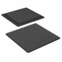
XC3SD3400A-4FGG676C Xilinx Inc, XC3SD3400A-4FGG676C Datasheet - Page 61

XC3SD3400A-4FGG676C
Manufacturer Part Number
XC3SD3400A-4FGG676C
Description
FPGA, SPARTAN-3A, DSP, 676FBGA
Manufacturer
Xilinx Inc
Series
Spartan™-3A DSPr
Datasheets
1.XC3S50A-4VQG100C.pdf
(7 pages)
2.XC3SD3400A-4FGG676C.pdf
(4 pages)
3.XC3SD3400A-4FGG676C.pdf
(101 pages)
Specifications of XC3SD3400A-4FGG676C
No. Of Logic Blocks
5968
No. Of Gates
3400000
No. Of Macrocells
53712
Family Type
Spartan-3A
No. Of Speed Grades
4
Total Ram Bits
2322432
No. Of I/o's
502
Clock Management
DCM
I/o Supply
RoHS Compliant
Number Of Logic Elements/cells
53712
Number Of Labs/clbs
5968
Number Of I /o
469
Number Of Gates
3400000
Voltage - Supply
1.14 V ~ 1.26 V
Mounting Type
Surface Mount
Operating Temperature
0°C ~ 85°C
Package / Case
676-BBGA
Package
676FBGA
Family Name
Spartan®-3A
Device Logic Units
53712
Device System Gates
3400000
Maximum Internal Frequency
667 MHz
Typical Operating Supply Voltage
1.2 V
Maximum Number Of User I/os
469
Ram Bits
2322432
Rohs Compliant
Yes
Lead Free Status / RoHS Status
Lead free / RoHS Compliant
For Use With
122-1532 - KIT DEVELOPMENT SPARTAN 3ADSP
Lead Free Status / RoHS Status
Lead free / RoHS Compliant
Other names
122-1539
Available stocks
Company
Part Number
Manufacturer
Quantity
Price
Company:
Part Number:
XC3SD3400A-4FGG676C
Manufacturer:
XilinxInc
Quantity:
3 000
Company:
Part Number:
XC3SD3400A-4FGG676C
Manufacturer:
Xilinx Inc
Quantity:
10 000
Company:
Part Number:
XC3SD3400A-4FGG676C
Manufacturer:
XILINX
Quantity:
592
Part Number:
XC3SD3400A-4FGG676C
Manufacturer:
XILINX/赛灵思
Quantity:
20 000
Revision History
The following table shows the revision history for this document.
DS610 (v3.0) October 4, 2010
Product Specification
04/02/07
05/25/07
06/18/07
07/16/07
06/02/08
03/11/09
10/04/10
Date
Version
1.0.1
1.0
1.2
2.0
2.1
2.2
3.0
Initial Xilinx release.
Minor edits.
Updated for v1.29 production speed files. Noted banking rules in
DIFF_HSTL_I and DIFF_HSTL_III to
in
Table
Table
timing in
Added Low-power options and updated typical values for quiescent current in
timing in
Improved V
V
Coupling Effects when Interfacing Large-Swing Single-Ended Signals to User I/O Pins.” Reduced typical
I
LVCMOS12/15/18 and improved V
V
Switching Output
Read cycles is the only unique limit. Updated speed files to v1.31 in
Setup and Hold times with device-specific values in
Table
SSO value in
performance via SCD 4103 in
DSP48A Timing
FBUFG in
minimum frequency in
Figure 14
Guides. Updated links.
Changed typical quiescent current temperature from ambient to quiescent. Updated selected I/O standard
DC characteristics. Removed PCIX IOSTANDARD due to limited PCIX interface support. Added T
T
references to SCD 4103.
Added I
in
notes 5 and 6 in
CCINTQ
IOPID
IN
OH
Table
Table 8
to Recommended Operating Conditions in
min to V
28. Updated DSP48A timing symbols, descriptions, and values in
45. Added CCLK specifications for Commercial in
20. Updated IOB Propagation times with device-specific values in
to
IK
and I
13. Updated I/O Test Method values in
Table
Table 34
Table
to
and
to note potential leakage between pins of a differential pair. Added note 6 to
Table 32
CCAUXT
Table
CCO
CCAUXQ
Table
Table 54
51. Updated JTAG specifications in
21. Updated BPI configuration waveforms in
tables. Simplified DSP48A F
Table
–0.4V for LVCMOS15/18 in
Guidelines. Removed DNA_RETENTION limit of 10 years in
and
3. Updated description for V
and V
28. Improved F
for -4 speed grade. Updated CCLK output maximum period in
quiescent current values by 20%-44% in
Table 47.
Table
12. Corrected symbols for T
from falling edge to rising edge. Added references to Spartan-3 Generation User
CCO2T
35.
Table 32,Table
Spartan-3A DSP FPGA Family: DC and Switching Characteristics
POR minimum in
Replaced BPI with SPI specification descriptions in
www.xilinx.com
IH
BUFG
min to 0.7V for LVCMOS12 in
Table
for -4 to 334 MHz in
12,
Table
MAX
37,
IN
Table 7
Table
Table
in
Revision
Table 4
Table
to value with all registers used in
SUSPEND_GTS
Table
11. Added reference to V
Table 7
Table
13, and
26. Added Simultaneously Switching Output limits in
and added reference to XAPP459, “Eliminating I/O
38, and
Table 46
and updated V
56.
19. Added reference to Sample Window in
including adding note 4. Also, added note 2 to I
Figure 14
Table
Table
Table
Table
and T
Table 11
through
Table
32. Added references to 375 MHz
26. Updated TMDS DC characteristics
Table 16
9. Increased V
39. Added explanatory footnotes to
and updated
SUSPEND_GWE
CCO
Table
Table
10. Changed V
Table
and
POR levels in
CCAUX
34. Added power-on timing in
and elsewhere. Updated IOB
Table
21. Improved SSTL_18_II
Table 14
Table
48. Updated Slave Parallel
Table 46
Table
in
IL
Table
Table
9. Updated DSP48A
12. Added
max to 0.4V for
Simultaneously
in
Table
OL
since number of
Table
52. Corrected BPI
35. Improved
Figure
55. Removed
max to 0.4V and
to match
10. Updated
44.
10. Added
IOPI
and
L
61


