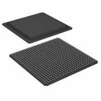
XC3SD3400A-4FGG676C Xilinx Inc, XC3SD3400A-4FGG676C Datasheet - Page 45

XC3SD3400A-4FGG676C
Manufacturer Part Number
XC3SD3400A-4FGG676C
Description
FPGA, SPARTAN-3A, DSP, 676FBGA
Manufacturer
Xilinx Inc
Series
Spartan™-3A DSPr
Datasheets
1.XC3S50A-4VQG100C.pdf
(7 pages)
2.XC3SD3400A-4FGG676C.pdf
(4 pages)
3.XC3SD3400A-4FGG676C.pdf
(101 pages)
Specifications of XC3SD3400A-4FGG676C
No. Of Logic Blocks
5968
No. Of Gates
3400000
No. Of Macrocells
53712
Family Type
Spartan-3A
No. Of Speed Grades
4
Total Ram Bits
2322432
No. Of I/o's
502
Clock Management
DCM
I/o Supply
RoHS Compliant
Number Of Logic Elements/cells
53712
Number Of Labs/clbs
5968
Number Of I /o
469
Number Of Gates
3400000
Voltage - Supply
1.14 V ~ 1.26 V
Mounting Type
Surface Mount
Operating Temperature
0°C ~ 85°C
Package / Case
676-BBGA
Package
676FBGA
Family Name
Spartan®-3A
Device Logic Units
53712
Device System Gates
3400000
Maximum Internal Frequency
667 MHz
Typical Operating Supply Voltage
1.2 V
Maximum Number Of User I/os
469
Ram Bits
2322432
Rohs Compliant
Yes
Lead Free Status / RoHS Status
Lead free / RoHS Compliant
For Use With
122-1532 - KIT DEVELOPMENT SPARTAN 3ADSP
Lead Free Status / RoHS Status
Lead free / RoHS Compliant
Other names
122-1539
Available stocks
Company
Part Number
Manufacturer
Quantity
Price
Company:
Part Number:
XC3SD3400A-4FGG676C
Manufacturer:
XilinxInc
Quantity:
3 000
Company:
Part Number:
XC3SD3400A-4FGG676C
Manufacturer:
Xilinx Inc
Quantity:
10 000
Company:
Part Number:
XC3SD3400A-4FGG676C
Manufacturer:
XILINX
Quantity:
592
Part Number:
XC3SD3400A-4FGG676C
Manufacturer:
XILINX/赛灵思
Quantity:
20 000
Table 37: Switching Characteristics for the DLL
DS610 (v3.0) October 4, 2010
Product Specification
Output Frequency Ranges
CLKOUT_FREQ_CLK0
CLKOUT_FREQ_CLK90
CLKOUT_FREQ_2X
CLKOUT_FREQ_DV
Output Clock Jitter
CLKOUT_PER_JITT_0
CLKOUT_PER_JITT_90
CLKOUT_PER_JITT_180
CLKOUT_PER_JITT_270
CLKOUT_PER_JITT_2X
CLKOUT_PER_JITT_DV1
CLKOUT_PER_JITT_DV2
Duty Cycle
CLKOUT_DUTY_CYCLE_
DLL
Phase Alignment
CLKIN_CLKFB_PHASE
CLKOUT_PHASE_DLL
Lock Time
LOCK_DLL
Symbol
(3)
(4)
(4)
(2)(3)(4)
Frequency for the CLK0 and CLK180 outputs
Frequency for the CLK90 and CLK270 outputs
Frequency for the CLK2X and CLK2X180 outputs
Frequency for the CLKDV output
Period jitter at the CLK0 output
Period jitter at the CLKDV output when performing
integer division
Period jitter at the CLKDV output when performing
non-integer division
Duty cycle variation for the CLK0, CLK90, CLK180,
CLK270, CLK2X, CLK2X180, and CLKDV outputs,
including the BUFGMUX and clock tree duty-cycle
distortion
outputs
When using the DLL alone:
The time from deassertion at
the DCM’s Reset input to the
rising transition at its LOCKED
output. When the DCM is
locked, the CLKIN and CLKFB
signals are in phase
Period jitter at the CLK90 output
Period jitter at the CLK180 output
Period jitter at the CLK270 output
Period jitter at the CLK2X and CLK2X180 outputs
Phase offset between the CLKIN and CLKFB inputs
Phase offset between DLL
Description
Spartan-3A DSP FPGA Family: DC and Switching Characteristics
www.xilinx.com
5 MHz < FCLKIN <
FCLKIN > 15 MHz
(not CLK2X180)
CLK0 to CLK2X
All others
15 MHz
Device
All
All
All
All
All
0.3125
Min
10
5
5
–
–
–
–
–
–
–
–
–
–
–
–
–
-5
±[1% of
±[1% of
±[1% of
±[0.5%
±[0.5%
CLKIN
CLKIN
CLKIN
CLKIN
CLKIN
period
+ 100]
period
+ 100]
period
+ 350]
period
+ 100]
period
+ 150]
±100
±150
±150
±150
±150
±150
Speed Grade
Max
280
200
334
186
600
of
of
5
0.3125
Min
10
5
5
–
–
–
–
–
–
–
–
–
–
–
–
–
-4
±[1% of
±[1% of
±[1% of
±[0.5%
±[0.5%
CLKIN
CLKIN
CLKIN
CLKIN
CLKIN
period
+ 100]
period
+ 100]
period
+ 350]
period
+ 100]
period
+ 150]
±100
±150
±150
±150
±150
±150
Max
250
200
334
166
600
of
of
5
Units
MHz
MHz
MHz
MHz
ms
ps
ps
ps
ps
ps
ps
ps
ps
ps
ps
ps
µs
45


