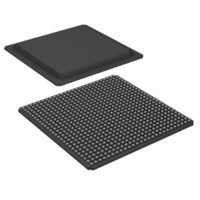
XC3SD3400A-4FGG676C Xilinx Inc, XC3SD3400A-4FGG676C Datasheet - Page 58

XC3SD3400A-4FGG676C
Manufacturer Part Number
XC3SD3400A-4FGG676C
Description
FPGA, SPARTAN-3A, DSP, 676FBGA
Manufacturer
Xilinx Inc
Series
Spartan™-3A DSPr
Datasheets
1.XC3S50A-4VQG100C.pdf
(7 pages)
2.XC3SD3400A-4FGG676C.pdf
(4 pages)
3.XC3SD3400A-4FGG676C.pdf
(101 pages)
Specifications of XC3SD3400A-4FGG676C
No. Of Logic Blocks
5968
No. Of Gates
3400000
No. Of Macrocells
53712
Family Type
Spartan-3A
No. Of Speed Grades
4
Total Ram Bits
2322432
No. Of I/o's
502
Clock Management
DCM
I/o Supply
RoHS Compliant
Number Of Logic Elements/cells
53712
Number Of Labs/clbs
5968
Number Of I /o
469
Number Of Gates
3400000
Voltage - Supply
1.14 V ~ 1.26 V
Mounting Type
Surface Mount
Operating Temperature
0°C ~ 85°C
Package / Case
676-BBGA
Package
676FBGA
Family Name
Spartan®-3A
Device Logic Units
53712
Device System Gates
3400000
Maximum Internal Frequency
667 MHz
Typical Operating Supply Voltage
1.2 V
Maximum Number Of User I/os
469
Ram Bits
2322432
Rohs Compliant
Yes
Lead Free Status / RoHS Status
Lead free / RoHS Compliant
For Use With
122-1532 - KIT DEVELOPMENT SPARTAN 3ADSP
Lead Free Status / RoHS Status
Lead free / RoHS Compliant
Other names
122-1539
Available stocks
Company
Part Number
Manufacturer
Quantity
Price
Company:
Part Number:
XC3SD3400A-4FGG676C
Manufacturer:
XilinxInc
Quantity:
3 000
Company:
Part Number:
XC3SD3400A-4FGG676C
Manufacturer:
Xilinx Inc
Quantity:
10 000
Company:
Part Number:
XC3SD3400A-4FGG676C
Manufacturer:
XILINX
Quantity:
592
Part Number:
XC3SD3400A-4FGG676C
Manufacturer:
XILINX/赛灵思
Quantity:
20 000
Byte Peripheral Interface (BPI) Configuration Timing
X-Ref Target - Figure 14
(Open-Drain)
Table 54: Timing for Byte-wide Peripheral Interface (BPI) Configuration Mode
DS610 (v3.0) October 4, 2010
Product Specification
T
T
T
T
T
T
T
T
CCLK1
CCLKn
MINIT
INITM
INITADDR
CCO
DCC
CCD
Symbol
PROG_B
LDC[2:0]
PUDC_B
CSO_B
A[25:0]
INIT_B
(Input)
(Input)
(Input)
(Input)
M[2:0]
D[7:0]
CCLK
HDC
Shaded values indicate specifications on attached parallel NOR Flash PROM.
Initial CCLK clock period
CCLK clock period after FPGA loads ConfigRate setting
Setup time on M[2:0] mode pins before the rising edge of INIT_B
Hold time on M[2:0] mode pins after the rising edge of INIT_B
Minimum period of initial A[25:0] address cycle; LDC[2:0] and HDC are asserted
and valid
Address A[25:0] outputs valid after CCLK falling edge
Setup time on D[7:0] data inputs before CCLK rising edge
Hold time on D[7:0] data inputs after CCLK rising edge
Figure 14: Waveforms for Byte-wide Peripheral Interface (BPI) Configuration
T
MINIT
<0:1:0>
PUDC_B must be stable before INIT_B goes High and constant throughout the configuration process.
T
INITM
Pin initially pulled High by internal pull-up resistor if PUDC_B input is Low.
Pin initially high-impedance (Hi-Z) if PUDC_B input is High.
Description
000_0000
T
CCLK1
Byte 0
Spartan-3A DSP FPGA Family: DC and Switching Characteristics
www.xilinx.com
Mode input pins M[2:0] are sampled when INIT_B goes High. After this point,
input values do not matter until DONE goes High, at which point the mode pins
become user-I/O pins.
T
INITADDR
000_0001
Byte 1
T
AVQV
Data
New ConfigRate active
Minimum
T
CCLK1
Address
T
50
CCO
0
0
5
Data
See T
T
DCC
See
See
See
SMDCC
T
Address
CCLKn
Maximum
Table 46
Table 46
Table 50
Data
in
–
–
5
–
Table 51
Address
DS529-3_05_090610
T
Data
CCD
T
cycles
Units
CCLK1
ns
ns
ns
58


