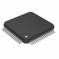
DS26502L+ Maxim Integrated Products, DS26502L+ Datasheet - Page 30

DS26502L+
Manufacturer Part Number
DS26502L+
Description
IC T1/E1/J1 64KCC ELEMENT 64LQFP
Manufacturer
Maxim Integrated Products
Type
BITS Elementr
Datasheet
1.DS26502LN.pdf
(125 pages)
Specifications of DS26502L+
Voltage - Supply
3.135 V ~ 3.465 V
Operating Temperature
0°C ~ 70°C
Mounting Type
Surface Mount
Package / Case
64-LQFP
Lead Free Status / RoHS Status
Lead free / RoHS Compliant
Frequency-max
-
Output
-
Input
-
- Current page: 30 of 125
- Download datasheet (4Mb)
7. PROCESSOR INTERFACE
The DS26502 is controlled via a nonmultiplexed (BIS[1:0] = 01) or a multiplexed (BIS[1:0] = 00)
parallel bus. There is also a serial bus mode option, as well as a hardware mode of operation. The bus
interface type is selected by BIS1 and BIS0 as shown in
Table 7-1. Port Mode Select
7.1 Parallel Port Functional Description
In parallel mode, the DS26502 can operate with either Intel or Motorola bus timing configurations. If the
BTS pin is tied low, Intel timing will be selected; if tied high, Motorola timing will be selected. All
Motorola bus signals are listed in parentheses (). See the timing diagrams in the AC Electrical
Characteristics section for more details.
7.2 SPI Serial Port Interface Functional Description
A serial SPI bus interface is selected when bus select is 10 (BIS[1:0] = 10). In this mode, a master/slave
relationship is enabled on the serial port with three signal lines (SCK, MOSI and MISO) and a chip select
(CS), with the DS26502 acting as the slave. Port read/write timing is not related to the system read/write
timing, thus allowing asynchronous, half-duplex operation. See the AC Electrical Characteristics section
for the AC timing characteristics of the serial port.
7.2.1 Clock Phase and Polarity
Clock Phase and Polarity are selected by the CPHA and CPOL pins. The slave device should always be
configured to match the bus master. See the
diagrams.
7.2.2 Bit Order
The most significant bit (MSB) of each byte is transmitted first.
7.2.3 Control Byte
The bus master will transmit two control bytes following a chip select to a slave device. The MSB will be
a R/W bit (1=read, 0=write). The next 6 bits will be padded with 0s. The LSB of the first byte will be
A[7]. The second control byte will be the address bits (A[6:0]) of the target register, followed by a Burst
bit in the LSB position (1=Burst, 0=Non-burst).
7.2.4 Burst Mode
The last bit of the second control byte (LSB) is the Burst mode bit. When the Burst bit is enabled (set to
1) and a read operation is performed, the register address is automatically incremented after the LSB of
the previous byte read to the next register address. Data will be available on the next clock edge following
the LSB of the previous byte read. When the Burst bit is enabled (set to 1) and a write operation is
performed, the register address will be automatically incremented to the next byte boundary following the
LSB of the previous register write, and 8 more data bits will be expected on the serial bus. Burst accesses
BIS1
0
0
1
1
BIS0
0
1
0
1
Parallel Port Mode (Multiplexed)
Parallel Port Mode (Nonmultiplexed)
Serial Port Mode (SPI)
Hardware Mode
PORT MODE
SPI Serial Port Mode
30 of 125
Table
7-1.
section for detailed functional timing
Related parts for DS26502L+
Image
Part Number
Description
Manufacturer
Datasheet
Request
R

Part Number:
Description:
MAX7528KCWPMaxim Integrated Products [CMOS Dual 8-Bit Buffered Multiplying DACs]
Manufacturer:
Maxim Integrated Products
Datasheet:

Part Number:
Description:
Single +5V, fully integrated, 1.25Gbps laser diode driver.
Manufacturer:
Maxim Integrated Products
Datasheet:

Part Number:
Description:
Single +5V, fully integrated, 155Mbps laser diode driver.
Manufacturer:
Maxim Integrated Products
Datasheet:

Part Number:
Description:
VRD11/VRD10, K8 Rev F 2/3/4-Phase PWM Controllers with Integrated Dual MOSFET Drivers
Manufacturer:
Maxim Integrated Products
Datasheet:

Part Number:
Description:
Highly Integrated Level 2 SMBus Battery Chargers
Manufacturer:
Maxim Integrated Products
Datasheet:

Part Number:
Description:
Current Monitor and Accumulator with Integrated Sense Resistor; ; Temperature Range: -40°C to +85°C
Manufacturer:
Maxim Integrated Products

Part Number:
Description:
TSSOP 14/A�/RS-485 Transceivers with Integrated 100O/120O Termination Resis
Manufacturer:
Maxim Integrated Products

Part Number:
Description:
TSSOP 14/A�/RS-485 Transceivers with Integrated 100O/120O Termination Resis
Manufacturer:
Maxim Integrated Products

Part Number:
Description:
QFN 16/A�/AC-DC and DC-DC Peak-Current-Mode Converters with Integrated Step
Manufacturer:
Maxim Integrated Products

Part Number:
Description:
TDFN/A/65V, 1A, 600KHZ, SYNCHRONOUS STEP-DOWN REGULATOR WITH INTEGRATED SWI
Manufacturer:
Maxim Integrated Products

Part Number:
Description:
Integrated Temperature Controller f
Manufacturer:
Maxim Integrated Products

Part Number:
Description:
SOT23-6/I�/45MHz to 650MHz, Integrated IF VCOs with Differential Output
Manufacturer:
Maxim Integrated Products

Part Number:
Description:
SOT23-6/I�/45MHz to 650MHz, Integrated IF VCOs with Differential Output
Manufacturer:
Maxim Integrated Products

Part Number:
Description:
EVALUATION KIT/2.4GHZ TO 2.5GHZ 802.11G/B RF TRANSCEIVER WITH INTEGRATED PA
Manufacturer:
Maxim Integrated Products

Part Number:
Description:
QFN/E/DUAL PCIE/SATA HIGH SPEED SWITCH WITH INTEGRATED BIAS RESISTOR
Manufacturer:
Maxim Integrated Products
Datasheet:


