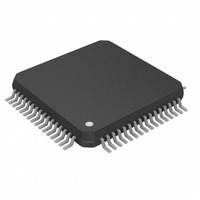
DS26502L+ Maxim Integrated Products, DS26502L+ Datasheet - Page 79

DS26502L+
Manufacturer Part Number
DS26502L+
Description
IC T1/E1/J1 64KCC ELEMENT 64LQFP
Manufacturer
Maxim Integrated Products
Type
BITS Elementr
Datasheet
1.DS26502LN.pdf
(125 pages)
Specifications of DS26502L+
Voltage - Supply
3.135 V ~ 3.465 V
Operating Temperature
0°C ~ 70°C
Mounting Type
Surface Mount
Package / Case
64-LQFP
Lead Free Status / RoHS Status
Lead free / RoHS Compliant
Frequency-max
-
Output
-
Input
-
- Current page: 79 of 125
- Download datasheet (4Mb)
13.2.2 Receive G.703 Section 13 Synchronization Signal
The DS26502 can receive a 2.048MHz square-wave synchronization clock as specified in Section 13 of
ITU G.703. To use the DS26502 in this mode, set the mode configuration bits in the Mode Configuration
Register (MCREG).
13.2.3 Monitor Mode
Monitor applications in both E1 and T1 require various flat gain settings for the receive-side circuitry.
The DS26502 can be programmed to support these applications via the monitor mode control bits MM1
and MM0 in the LIC3 register.
Figure 13-2. Typical Monitor Application
13.3 LIU Transmitter
The DS26502 uses a phase-lock loop along with a precision digital-to-analog converter (DAC) to create
the waveforms that are transmitted onto the E1 or T1 line. The waveforms created by the DS26502 meet
the latest ETSI, ITU, ANSI, and AT&T specifications. The waveform that is to be generated is set by the
transmit mode bits (TMODE[3:0]) in the MCREG register, as well as the L2/L1/L0 bits in register LIC1
if applicable.
ITU specification G.703 requires an accuracy of ±50ppm for both T1 and E1. TR62411 and ANSI specs
require an accuracy of ±32ppm for T1 interfaces. The transmit clock can be sourced from the recovered
clock (RCLK), the pre-scaled MCLK, the TCLK pin or the TX PLL. See the TX PLL clock mux diagram
in
0.005UI
source. Also, the waveforms created are independent of the duty cycle of TCLK. The transmitter in the
DS26502 couples to the transmit twisted pair (or coaxial cable in some applications) via a 1:2 step-up
transformer. For the device to create the proper waveforms, the transformer used must meet the
specifications listed in
termination.
Figure
P-P
T1/E1 LINE
3-3. Due to the nature of the design of the transmitter in the DS26502, very little jitter (less than
broadband from 10Hz to 100kHz) is added to the jitter present on the selected transmit clock
Rm
Table
MONITOR
PORT JACK
Rm
13-1. The DS26502 has the option of using software-selectable transmit
PRIMARY
T1/E1 TERMINATING
DEVICE
79 of 125
X
F
M
R
SECONDARY T1/E1
TERMINATING
DEVICE
Rt
DS26502
Related parts for DS26502L+
Image
Part Number
Description
Manufacturer
Datasheet
Request
R

Part Number:
Description:
MAX7528KCWPMaxim Integrated Products [CMOS Dual 8-Bit Buffered Multiplying DACs]
Manufacturer:
Maxim Integrated Products
Datasheet:

Part Number:
Description:
Single +5V, fully integrated, 1.25Gbps laser diode driver.
Manufacturer:
Maxim Integrated Products
Datasheet:

Part Number:
Description:
Single +5V, fully integrated, 155Mbps laser diode driver.
Manufacturer:
Maxim Integrated Products
Datasheet:

Part Number:
Description:
VRD11/VRD10, K8 Rev F 2/3/4-Phase PWM Controllers with Integrated Dual MOSFET Drivers
Manufacturer:
Maxim Integrated Products
Datasheet:

Part Number:
Description:
Highly Integrated Level 2 SMBus Battery Chargers
Manufacturer:
Maxim Integrated Products
Datasheet:

Part Number:
Description:
Current Monitor and Accumulator with Integrated Sense Resistor; ; Temperature Range: -40°C to +85°C
Manufacturer:
Maxim Integrated Products

Part Number:
Description:
TSSOP 14/A�/RS-485 Transceivers with Integrated 100O/120O Termination Resis
Manufacturer:
Maxim Integrated Products

Part Number:
Description:
TSSOP 14/A�/RS-485 Transceivers with Integrated 100O/120O Termination Resis
Manufacturer:
Maxim Integrated Products

Part Number:
Description:
QFN 16/A�/AC-DC and DC-DC Peak-Current-Mode Converters with Integrated Step
Manufacturer:
Maxim Integrated Products

Part Number:
Description:
TDFN/A/65V, 1A, 600KHZ, SYNCHRONOUS STEP-DOWN REGULATOR WITH INTEGRATED SWI
Manufacturer:
Maxim Integrated Products

Part Number:
Description:
Integrated Temperature Controller f
Manufacturer:
Maxim Integrated Products

Part Number:
Description:
SOT23-6/I�/45MHz to 650MHz, Integrated IF VCOs with Differential Output
Manufacturer:
Maxim Integrated Products

Part Number:
Description:
SOT23-6/I�/45MHz to 650MHz, Integrated IF VCOs with Differential Output
Manufacturer:
Maxim Integrated Products

Part Number:
Description:
EVALUATION KIT/2.4GHZ TO 2.5GHZ 802.11G/B RF TRANSCEIVER WITH INTEGRATED PA
Manufacturer:
Maxim Integrated Products

Part Number:
Description:
QFN/E/DUAL PCIE/SATA HIGH SPEED SWITCH WITH INTEGRATED BIAS RESISTOR
Manufacturer:
Maxim Integrated Products
Datasheet:


