DS26502L+ Maxim Integrated Products, DS26502L+ Datasheet - Page 37
DS26502L+
Manufacturer Part Number
DS26502L+
Description
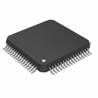
IC T1/E1/J1 64KCC ELEMENT 64LQFP
Manufacturer
Maxim Integrated Products
Type
BITS Elementr
Datasheet
1.DS26502LN.pdf
(125 pages)
Specifications of DS26502L+
Voltage - Supply
3.135 V ~ 3.465 V
Operating Temperature
0°C ~ 70°C
Mounting Type
Surface Mount
Package / Case
64-LQFP
Lead Free Status / RoHS Status
Lead free / RoHS Compliant
Frequency-max
-
Output
-
Input
-


Register Name:
Register Description:
Register Address:
Bit #
Name
Default
HW
Mode
For more information on all the bits in the Transmit PLL control register, refer to
Bits 0 and 1: Transmit Clock (TX CLOCK) Source Select (TCSS[1:0]). These bits control the output of the TX PLL
Clock Mux function. See
Bit 2: Transmit PLL_CLK Source Select (TPLLSS). Selects the reference signal for the TX PLL.
Bit 3 and 4: Transmit PLL Input Frequency Select (TPLLIFS[0:1]). These bits are used to indicate the reference
frequency being input to the TX PLL.
Bit 5: PLL_OUT Select (PLLOS). This bit selects the source for the PLL_OUT pin. See
Bits 6 and 7: Transmit PLL Output Frequency Select (TPLLOFS[1:0]). These bits are used to select the TX PLL output
frequency.
TPLLIFS1
TPLLOFS1
TCSS1
0
0
1
1
0
0
1
1
0
0
1
1
0 = Use the recovered network clock. This is the same clock available at the RCLK pin (output).
1 = Use the externally provided clock present at the TCLK pin.
0 = PLL_OUT is sourced directly from the TX PLL.
1 = PLL_OUT is the output of the TX PLL mux.
TPLLOFS1
TCSS0
TPLLIFS0
TPLLOFS0
7
0
0
0
1
0
1
0
1
0
1
0
1
0
1
Figure
TPLLOFS0
TPCR
Transmit PLL Control Register
09h
The TCLK pin is the source of transmit clock.
The PLL_CLK is the source of transmit clock.
The scaled signal present at MCLK as the transmit clock.
The signal present at RCLK is the transmit clock.
6
0
0
3-3.
Output Frequency
Input Frequency
1.544MHz
2.048MHz
1.544MHz
2.048MHz
6312kHz
6312kHz
PLLOS
64kHz
64kHz
5
0
0
Transmit Clock (TX CLOCK) Source
TPLLIFS1
37 of 125
4
0
0
(See
Figure
TPLLIFS0
3-3)
3
0
0
Figure
TPLLSS
2
0
0
3-3.
Figure
TCSS1
TCSS1
PIN 31
3-3.
1
0
TCSS0
TCSS0
PIN 63
0
0
Related parts for DS26502L+
Image
Part Number
Description
Manufacturer
Datasheet
Request
R

Part Number:
Description:
MAX7528KCWPMaxim Integrated Products [CMOS Dual 8-Bit Buffered Multiplying DACs]
Manufacturer:
Maxim Integrated Products
Datasheet:
Part Number:
Description:
Single +5V, fully integrated, 1.25Gbps laser diode driver.
Manufacturer:
Maxim Integrated Products
Datasheet:
Part Number:
Description:
Single +5V, fully integrated, 155Mbps laser diode driver.
Manufacturer:
Maxim Integrated Products
Datasheet:
Part Number:
Description:
VRD11/VRD10, K8 Rev F 2/3/4-Phase PWM Controllers with Integrated Dual MOSFET Drivers
Manufacturer:
Maxim Integrated Products
Datasheet:
Part Number:
Description:
Highly Integrated Level 2 SMBus Battery Chargers
Manufacturer:
Maxim Integrated Products
Datasheet:
Part Number:
Description:
Current Monitor and Accumulator with Integrated Sense Resistor; ; Temperature Range: -40°C to +85°C
Manufacturer:
Maxim Integrated Products
Part Number:
Description:
TSSOP 14/A�/RS-485 Transceivers with Integrated 100O/120O Termination Resis
Manufacturer:
Maxim Integrated Products
Part Number:
Description:
TSSOP 14/A�/RS-485 Transceivers with Integrated 100O/120O Termination Resis
Manufacturer:
Maxim Integrated Products
Part Number:
Description:
QFN 16/A�/AC-DC and DC-DC Peak-Current-Mode Converters with Integrated Step
Manufacturer:
Maxim Integrated Products
Part Number:
Description:
TDFN/A/65V, 1A, 600KHZ, SYNCHRONOUS STEP-DOWN REGULATOR WITH INTEGRATED SWI
Manufacturer:
Maxim Integrated Products
Part Number:
Description:
Integrated Temperature Controller f
Manufacturer:
Maxim Integrated Products
Part Number:
Description:
SOT23-6/I�/45MHz to 650MHz, Integrated IF VCOs with Differential Output
Manufacturer:
Maxim Integrated Products
Part Number:
Description:
SOT23-6/I�/45MHz to 650MHz, Integrated IF VCOs with Differential Output
Manufacturer:
Maxim Integrated Products
Part Number:
Description:
EVALUATION KIT/2.4GHZ TO 2.5GHZ 802.11G/B RF TRANSCEIVER WITH INTEGRATED PA
Manufacturer:
Maxim Integrated Products
Part Number:
Description:
QFN/E/DUAL PCIE/SATA HIGH SPEED SWITCH WITH INTEGRATED BIAS RESISTOR
Manufacturer:
Maxim Integrated Products
Datasheet: