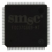
FDC37C669-MT SMSC, FDC37C669-MT Datasheet - Page 23

FDC37C669-MT
Manufacturer Part Number
FDC37C669-MT
Description
IC CTRLR SUPER I/O FLPPY 100TQFP
Manufacturer
SMSC
Datasheet
1.FDC37C669-MT.pdf
(162 pages)
Specifications of FDC37C669-MT
Controller Type
I/O Controller
Interface
ISA Host
Voltage - Supply
4.5 V ~ 5.5 V
Current - Supply
25mA
Operating Temperature
0°C ~ 70°C
Mounting Type
Surface Mount
Package / Case
100-TQFP, 100-VQFP
Lead Free Status / RoHS Status
Lead free / RoHS Compliant
Other names
638-1008
Available stocks
Company
Part Number
Manufacturer
Quantity
Price
Company:
Part Number:
FDC37C669-MT
Manufacturer:
Microchip Technology
Quantity:
10 000
- Current page: 23 of 162
- Download datasheet (619Kb)
DIGITAL OUTPUT REGISTER (DOR)
Address 3F2 READ/WRITE
The DOR controls the drive select and motor enables of
the disk interface outputs. It also
BIT 0 and 1 DRIVE SELECT
These two bit a are binary encoded for the four drive
selects DS0-DS3, thereby allowing only one drive to be
selected at one time.
BIT 2 nRESET
A logic "0" written to this bit resets the Floppy disk
controller. This reset will remain active until a logic "1" is
written to this bit. This software reset does not affect the
DSR and CCR registers, nor does it affect the other bits
of the DOR register.
required is 100ns, therefore toggling this bit by
consecutive writes to this register is a valid method of
issuing a software reset.
BIT 3 DMAEN
PC/AT and Model 30 Mode:
Writing this bit to logic "1" will enable the DRQ, nDACK,
TC and FINTR outputs. This bit being a logic "0" will
disable the nDACK and TC inputs, and hold the DRQ and
FINTR outputs in a high impedance state. This bit is a
logic "0" after a reset and in these modes.
PS/2 Mode: In this mode the DRQ, nDACK, TC and
FINTR pins are always enabled.
DRQ, nDACK, TC, and FINTR pins will remain enabled,
but this bit will be cleared to a logic "0".
RESET
COND.
MOT
EN3
7
0
The minimum reset duration
MOT
EN2
6
0
During a reset, the
MOT
EN1
5
0
MOT
EN0
4
0
DMAEN nRESET DRIVE
23
3
0
contains the enable for the DMA logic and contains a
software reset bit.
unaffected by a software reset. The DOR can be written
to at any time.
BIT 4 MOTOR ENABLE 0
This bit controls the MTR0 disk interface output. A logic
"1" in this bit will cause the output pin to go active.
BIT 5 MOTOR ENABLE 1
This bit controls the MTR1 disk interface output. A logic
"1" in this bit will cause the output pin to go active.
BIT 6 MOTOR ENABLE 2
This bit controls the MTR2 disk interface output. A logic
"1" in this bit will cause the output pin to go active.
BIT 7 MOTOR ENABLE 3
This bit controls the MTR3 disk interface output. A logic
"1" in this bit causes the output to go active.
Table 3 - Drive Activation Values
DRIVE
2
0
0
1
2
3
SEL1
1
0
The contents of the DOR are
DRIVE
SEL0
DOR VALUE
0
0
1CH
2DH
4EH
8FH
Related parts for FDC37C669-MT
Image
Part Number
Description
Manufacturer
Datasheet
Request
R

Part Number:
Description:
FAST ETHERNET PHYSICAL LAYER DEVICE
Manufacturer:
SMSC Corporation
Datasheet:

Part Number:
Description:
357-036-542-201 CARDEDGE 36POS DL .156 BLK LOPRO
Manufacturer:
SMSC Corporation
Datasheet:

Part Number:
Description:
357-036-542-201 CARDEDGE 36POS DL .156 BLK LOPRO
Manufacturer:
SMSC Corporation
Datasheet:

Part Number:
Description:
357-036-542-201 CARDEDGE 36POS DL .156 BLK LOPRO
Manufacturer:
SMSC Corporation
Datasheet:

Part Number:
Description:
4-PORT USB2.0 HUB CONTROLLER
Manufacturer:
SMSC Corporation
Datasheet:

Part Number:
Description:
Manufacturer:
SMSC Corporation
Datasheet:

Part Number:
Description:
Manufacturer:
SMSC Corporation
Datasheet:

Part Number:
Description:
FDC37C672ENHANCED SUPER I/O CONTROLLER WITH FAST IR
Manufacturer:
SMSC Corporation
Datasheet:

Part Number:
Description:
COM90C66LJPARCNET Controller/Transceiver with AT Interface and On-Chip RAM
Manufacturer:
SMSC Corporation
Datasheet:

Part Number:
Description:
Manufacturer:
SMSC Corporation
Datasheet:

Part Number:
Description:
Manufacturer:
SMSC Corporation
Datasheet:

Part Number:
Description:
Manufacturer:
SMSC Corporation
Datasheet:

Part Number:
Description:
Manufacturer:
SMSC Corporation
Datasheet:


