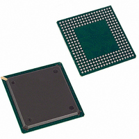
DS33R11+ Maxim Integrated Products, DS33R11+ Datasheet - Page 300

DS33R11+
Manufacturer Part Number
DS33R11+
Description
IC ETH TXRX T1/E1/J1 256-BGA
Manufacturer
Maxim Integrated Products
Type
Transceiverr
Datasheet
1.DS33R11.pdf
(344 pages)
Specifications of DS33R11+
Protocol
T1/E1/J1
Voltage - Supply
1.8V, 3.3V
Mounting Type
Surface Mount
Package / Case
256-BGA
Lead Free Status / RoHS Status
Lead free / RoHS Compliant
Number Of Drivers/receivers
-
- Current page: 300 of 344
- Download datasheet (12Mb)
12 FUNCTIONAL TIMING
12.1 Functional Serial I/O Timing
The Serial Interface provides flexible timing to interconnect with a wide variety of serial interfaces. TDEN is an
input signal that can be used to enable or block the TSERO data. The “shaded bits” are not clocked by the
DS33R11. The TDEN must occur one bit before the effected bit in the TSERO stream. Note that polarity of the
TDEN is selectable through LI.TSLCR. In the figure below, TDEN is active low, allowing the bits to clock and
inactive high, causing the next data bit not be clocked. TCLKE can be gapped as shown in the following figure.
Similarly, the receiver function is governed by RCLKI, RDEN and RSERI. RSERI data will not be provided to the
receiver for the bits blocked when RDEN is inactive. The RDEN polarity can be programmed by LI.RSLCR. The
RDEN signal must be coincident with the RSERI bit that needs to be blocked.
Figure 12-1. Tx Serial Interface Functional Timing
Figure 12-2. Rx Serial Interface Functional Timing
RCLKI Gapped
TCLKE Gapped
TSERO
RSERI
TSER
gapped
TSER
TSERO
RSERI
TCLKE
RCLKI
RDEN
TCLK
TDEN
300 of 344
Related parts for DS33R11+
Image
Part Number
Description
Manufacturer
Datasheet
Request
R

Part Number:
Description:
MAX7528KCWPMaxim Integrated Products [CMOS Dual 8-Bit Buffered Multiplying DACs]
Manufacturer:
Maxim Integrated Products
Datasheet:

Part Number:
Description:
Single +5V, fully integrated, 1.25Gbps laser diode driver.
Manufacturer:
Maxim Integrated Products
Datasheet:

Part Number:
Description:
Single +5V, fully integrated, 155Mbps laser diode driver.
Manufacturer:
Maxim Integrated Products
Datasheet:

Part Number:
Description:
VRD11/VRD10, K8 Rev F 2/3/4-Phase PWM Controllers with Integrated Dual MOSFET Drivers
Manufacturer:
Maxim Integrated Products
Datasheet:

Part Number:
Description:
Highly Integrated Level 2 SMBus Battery Chargers
Manufacturer:
Maxim Integrated Products
Datasheet:

Part Number:
Description:
Current Monitor and Accumulator with Integrated Sense Resistor; ; Temperature Range: -40°C to +85°C
Manufacturer:
Maxim Integrated Products

Part Number:
Description:
TSSOP 14/A�/RS-485 Transceivers with Integrated 100O/120O Termination Resis
Manufacturer:
Maxim Integrated Products

Part Number:
Description:
TSSOP 14/A�/RS-485 Transceivers with Integrated 100O/120O Termination Resis
Manufacturer:
Maxim Integrated Products

Part Number:
Description:
QFN 16/A�/AC-DC and DC-DC Peak-Current-Mode Converters with Integrated Step
Manufacturer:
Maxim Integrated Products

Part Number:
Description:
TDFN/A/65V, 1A, 600KHZ, SYNCHRONOUS STEP-DOWN REGULATOR WITH INTEGRATED SWI
Manufacturer:
Maxim Integrated Products

Part Number:
Description:
Integrated Temperature Controller f
Manufacturer:
Maxim Integrated Products

Part Number:
Description:
SOT23-6/I�/45MHz to 650MHz, Integrated IF VCOs with Differential Output
Manufacturer:
Maxim Integrated Products

Part Number:
Description:
SOT23-6/I�/45MHz to 650MHz, Integrated IF VCOs with Differential Output
Manufacturer:
Maxim Integrated Products

Part Number:
Description:
EVALUATION KIT/2.4GHZ TO 2.5GHZ 802.11G/B RF TRANSCEIVER WITH INTEGRATED PA
Manufacturer:
Maxim Integrated Products

Part Number:
Description:
QFN/E/DUAL PCIE/SATA HIGH SPEED SWITCH WITH INTEGRATED BIAS RESISTOR
Manufacturer:
Maxim Integrated Products
Datasheet:


