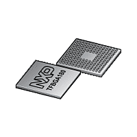
LPC3130_3131 NXP Semiconductors, LPC3130_3131 Datasheet - Page 6

LPC3130_3131
Manufacturer Part Number
LPC3130_3131
Description
The NXP LPC3130/3131 combine an 180 MHz ARM926EJ-S CPU core, high-speed USB2
Manufacturer
NXP Semiconductors
Datasheet
1.LPC3130_3131.pdf
(68 pages)
- Current page: 6 of 68
- Download datasheet (301Kb)
NXP Semiconductors
Table 3.
Table 4.
Pin names with prefix m are multiplexed pins. See
LPC3130_3131_1
Preliminary data sheet
Pin Symbol
Row P
1
5
9
13
Pin name
Clock Generation Unit
FFAST_IN
FFAST_OUT
VDDA12
VSSA12
RSTIN_N
CLK_256FS_O
CLOCK_OUT
SYSCLK_O
10-bit ADC
ADC10B_VDDA33
ADC10B_GNDA
ADC10B_GPA0
ADC10B_GPA1
ADC10B_GPA2
ADC10B_GPA3
USB HS 2.0 OTG
USB_VBUS
USB_ID
USB_RREF
USB_DP
USB_DM
USB_VDDA33
mLCD_DB_7
mLCD_DB_1
TRST_N
Pin allocation table
Pin description
[3]
BGA
Ball
A10
B10
D11;
E10
E9
H14
H12
J4
G13
A13
A12
B14
A14
B13
C14
L2
M1
J5
P2
N2
Pin Symbol
2
6
10
14
…continued
Digital
I/O
level
[1]
SUP1
SUP1
SUP1
SUP3
SUP3
SUP3
SUP3
SUP3
SUP3
SUP3
SUP3
SUP3
SUP5
SUP3
SUP3
SUP3
SUP3
USB_DP
mLCD_DB_3
TMS
mUART_RTS_N
Application
function
AI
AO
Supply
Ground
DI
DO
DO
DO
Supply
Ground
AI
AI
AI
AI
AI
AI
AIO
AIO
AIO
Rev. 1 — 9 February 2009
Table 10
Pin
state
after
reset
-
-
I
O
O
O
-
-
-
-
-
-
-
-
-
-
-
for pin function selection of multiplexed pins.
Pin Symbol
3
7
11
-
Low-cost, low-power ARM926EJ-S microcontrollers
Cell
Type
AIO2
AIO2
PS3
CG1
DIO2
DIO1
DIO1
DIO1
PS3
CG1
AIO1
AIO1
AIO1
AIO1
AIO3
AIO1
AIO1
AIO1
AIO1
mLCD_DB_14
mLCD_DB_5
I2SRX_WS0
-
[2]
Description
12 MHz oscillator clock input
12 MHz oscillator clock output
12 MHz oscillator/PLLs Analog supply
12 MHz oscillator/PLLs Analog ground
System Reset Input (active LOW)
Programmable clock output; fractionally
derived from CLK1024FS_BASE clock
domain. Generally used for Audio Codec
master clock.
Programmable clock output; fractionally
derived from SYS_BASE clock domain.
Programmable clock output. Output one of
seven base/reference input clocks. No
fractional divider.
10-bit ADC Analog Supply
10-bit ADC Analog Ground
10-bit ADC Analog Input
10-bit ADC Analog Input
10-bit ADC Analog Input
10-bit ADC Analog Input
USB supply detection line
Indicates to the USB transceiver whether in
device (USB_ID HIGH) or host (USB_ID LOW)
mode (contains internal pull-up resistor)
USB Connection for external reference resistor
(12 k
USB D+ connection with integrated 45
termination resistor
USB D connection with integrated 45
termination resistor
1 %) to analog ground supply
LPC3130/3131
Pin Symbol
4
8
12
-
mLCD_DB_13
mLCD_RS
UART_RXD
-
© NXP B.V. 2009. All rights reserved.
6 of 68
Related parts for LPC3130_3131
Image
Part Number
Description
Manufacturer
Datasheet
Request
R

Part Number:
Description:
Manufacturer:
Philips Semiconductors (Acquired by NXP)
Datasheet:
Part Number:
Description:
NXP Semiconductors designed the LPC2420/2460 microcontroller around a 16-bit/32-bitARM7TDMI-S CPU core with real-time debug interfaces that include both JTAG andembedded trace
Manufacturer:
NXP Semiconductors
Datasheet:

Part Number:
Description:
NXP Semiconductors designed the LPC2458 microcontroller around a 16-bit/32-bitARM7TDMI-S CPU core with real-time debug interfaces that include both JTAG andembedded trace
Manufacturer:
NXP Semiconductors
Datasheet:
Part Number:
Description:
NXP Semiconductors designed the LPC2468 microcontroller around a 16-bit/32-bitARM7TDMI-S CPU core with real-time debug interfaces that include both JTAG andembedded trace
Manufacturer:
NXP Semiconductors
Datasheet:
Part Number:
Description:
NXP Semiconductors designed the LPC2470 microcontroller, powered by theARM7TDMI-S core, to be a highly integrated microcontroller for a wide range ofapplications that require advanced communications and high quality graphic displays
Manufacturer:
NXP Semiconductors
Datasheet:
Part Number:
Description:
NXP Semiconductors designed the LPC2478 microcontroller, powered by theARM7TDMI-S core, to be a highly integrated microcontroller for a wide range ofapplications that require advanced communications and high quality graphic displays
Manufacturer:
NXP Semiconductors
Datasheet:
Part Number:
Description:
The Philips Semiconductors XA (eXtended Architecture) family of 16-bit single-chip microcontrollers is powerful enough to easily handle the requirements of high performance embedded applications, yet inexpensive enough to compete in the market for hi
Manufacturer:
NXP Semiconductors
Datasheet:
Part Number:
Description:
The XA-S3 device is a member of Philips Semiconductors? XA(eXtended Architecture) family of high performance 16-bitsingle-chip microcontrollers
Manufacturer:
NXP Semiconductors
Datasheet:

Part Number:
Description:
The NXP BlueStreak LH75401/LH75411 family consists of two low-cost 16/32-bit System-on-Chip (SoC) devices
Manufacturer:
NXP Semiconductors
Datasheet:

Part Number:
Description:
The NXP LPC3141 combine a 270 MHz ARM926EJ-S CPU core, High-speed USB 2
Manufacturer:
NXP Semiconductors

Part Number:
Description:
The NXP LPC3143 combine a 270 MHz ARM926EJ-S CPU core, High-speed USB 2
Manufacturer:
NXP Semiconductors

Part Number:
Description:
The NXP LPC3152 combines an 180 MHz ARM926EJ-S CPU core, High-speed USB 2
Manufacturer:
NXP Semiconductors

Part Number:
Description:
The NXP LPC3154 combines an 180 MHz ARM926EJ-S CPU core, High-speed USB 2
Manufacturer:
NXP Semiconductors

Part Number:
Description:
Standard level N-channel enhancement mode Field-Effect Transistor (FET) in a plastic package using NXP High-Performance Automotive (HPA) TrenchMOS technology
Manufacturer:
NXP Semiconductors
Datasheet:


