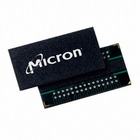
MT41J256M4HX-15E:D TR Micron Technology Inc, MT41J256M4HX-15E:D TR Datasheet - Page 120

MT41J256M4HX-15E:D TR
Manufacturer Part Number
MT41J256M4HX-15E:D TR
Description
IC DDR3 SDRAM 1GBIT 78FBGA
Manufacturer
Micron Technology Inc
Type
DDR3 SDRAMr
Specifications of MT41J256M4HX-15E:D TR
Format - Memory
RAM
Memory Type
DDR3 SDRAM
Memory Size
1G (256M x 4)
Speed
667MHz
Interface
Parallel
Voltage - Supply
1.425 V ~ 1.575 V
Operating Temperature
0°C ~ 95°C
Package / Case
78-FBGA
Organization
256Mx4
Density
1Gb
Address Bus
17b
Maximum Clock Rate
1.333GHz
Operating Supply Voltage (typ)
1.5V
Package Type
FBGA
Operating Temp Range
0C to 95C
Operating Supply Voltage (max)
1.575V
Operating Supply Voltage (min)
1.425V
Supply Current
220mA
Pin Count
78
Mounting
Surface Mount
Operating Temperature Classification
Commercial
Lead Free Status / RoHS Status
Lead free / RoHS Compliant
- Current page: 120 of 181
- Download datasheet (9Mb)
Figure 61: Multipurpose Register (MPR) Block Diagram
Table 69:
MPR Functional Description
PDF: 09005aef826aa906/Source: 09005aef82a357c3
1Gb_DDR3_4.fm - Rev. F 11/08 EN
MR3[2]
MPR
0
1
(see Table 70 on page 121)
MPR Functional Description of MR3 Bits
MPR READ Function
Notes:
“Don’t Care”
MR3[1:0]
A[1:0]
1. A predefined data pattern can be read out of the MPR with an external READ command.
2. MR3[2] defines whether the data flow comes from the memory core or the MPR. When the
The MPR JEDEC definition allows for either a prime DQ (DQ0 on a x4 and a x8; on a x16,
DQ0 = lower byte and DQ8 = upper byte) to output the MPR data with the remaining DQ
driven LOW or for all DQ to output the MPR data. The MPR readout supports fixed READ
burst and READ burst chop (MRS and OTF via A12/BC#) with regular READ latencies
and AC timings applicable, provided the DLL is locked as required.
MPR addressing for a valid MPR read is as follows:
• A[1:0] must be set to “00” as the burst order is fixed per nibble
• A2 selects the burst order:
• For burst chop 4 cases, the burst order is switched on the nibble base and:
• Burst order bit 0 (the first bit) is assigned to LSB, and burst order bit 7 (the last bit) is
• A[9:3] are a “Don’t Care”
• A10 is a “Don’t Care”
Memory core
– BL8, A2 is set to “0,” and the burst order is fixed to 0, 1, 2, 3, 4, 5, 6, 7
– A2 = 0; burst order = 0, 1, 2, 3
– A2 = 1; burst order = 4, 5, 6, 7
assigned to MSB
data flow is defined, the MPR contents can be read out continuously with a regular READ or
RDAP command.
DQ, DM, DQS, DQS#
Enable MPR mode, subsequent READ/RDAP commands defined by bits 1 and 2
MR3[2] = 1 (MPR on)
MR3[2] = 0 (MPR off)
All subsequent READs come from the DRAM memory array
All subsequent WRITEs go to the DRAM memory array
120
Normal operation, no MPR transaction
predefined data for READs
Multipurpose register
Micron Technology, Inc., reserves the right to change products or specifications without notice.
Function
1Gb: x4, x8, x16 DDR3 SDRAM
©2006 Micron Technology, Inc. All rights reserved.
Operations
Related parts for MT41J256M4HX-15E:D TR
Image
Part Number
Description
Manufacturer
Datasheet
Request
R

Part Number:
Description:
Manufacturer:
Micron Technology Inc
Datasheet:

Part Number:
Description:
Manufacturer:
Micron Technology Inc
Datasheet:

Part Number:
Description:
IC SDRAM 64MBIT 133MHZ 54TSOP
Manufacturer:
Micron Technology Inc
Datasheet:

Part Number:
Description:
IC SDRAM 64MBIT 5.5NS 86TSOP
Manufacturer:
Micron Technology Inc
Datasheet:

Part Number:
Description:
IC SDRAM 64MBIT 200MHZ 86TSOP
Manufacturer:
Micron Technology Inc
Datasheet:

Part Number:
Description:
IC SDRAM 64MBIT 133MHZ 54TSOP
Manufacturer:
Micron Technology Inc
Datasheet:

Part Number:
Description:
IC SDRAM 128MBIT 133MHZ 54TSOP
Manufacturer:
Micron Technology Inc
Datasheet:

Part Number:
Description:
IC SDRAM 256MBIT 133MHZ 90VFBGA
Manufacturer:
Micron Technology Inc
Datasheet:

Part Number:
Description:
IC SDRAM 128MBIT 133MHZ 54TSOP
Manufacturer:
Micron Technology Inc
Datasheet:

Part Number:
Description:
IC SDRAM 256MBIT 133MHZ 54TSOP
Manufacturer:
Micron Technology Inc
Datasheet:

Part Number:
Description:
IC DDR SDRAM 512MBIT 6NS 66TSOP
Manufacturer:
Micron Technology Inc
Datasheet:

Part Number:
Description:
IC SDRAM 128MBIT 167MHZ 86TSOP
Manufacturer:
Micron Technology Inc
Datasheet:

Part Number:
Description:
IC SDRAM 128MBIT 143MHZ 86TSOP
Manufacturer:
Micron Technology Inc
Datasheet:

Part Number:
Description:
SDRAM 256M-BIT 1.8V 54-PIN VFBGA
Manufacturer:
Micron Technology Inc
Datasheet:

Part Number:
Description:
IC SDRAM 128MBIT 143MHZ 86TSOP
Manufacturer:
Micron Technology Inc
Datasheet:


