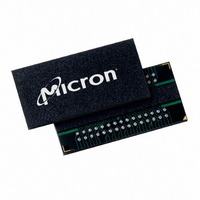
MT41J256M4HX-15E:D TR Micron Technology Inc, MT41J256M4HX-15E:D TR Datasheet - Page 127

MT41J256M4HX-15E:D TR
Manufacturer Part Number
MT41J256M4HX-15E:D TR
Description
IC DDR3 SDRAM 1GBIT 78FBGA
Manufacturer
Micron Technology Inc
Type
DDR3 SDRAMr
Specifications of MT41J256M4HX-15E:D TR
Format - Memory
RAM
Memory Type
DDR3 SDRAM
Memory Size
1G (256M x 4)
Speed
667MHz
Interface
Parallel
Voltage - Supply
1.425 V ~ 1.575 V
Operating Temperature
0°C ~ 95°C
Package / Case
78-FBGA
Organization
256Mx4
Density
1Gb
Address Bus
17b
Maximum Clock Rate
1.333GHz
Operating Supply Voltage (typ)
1.5V
Package Type
FBGA
Operating Temp Range
0C to 95C
Operating Supply Voltage (max)
1.575V
Operating Supply Voltage (min)
1.425V
Supply Current
220mA
Pin Count
78
Mounting
Surface Mount
Operating Temperature Classification
Commercial
Lead Free Status / RoHS Status
Lead free / RoHS Compliant
- Current page: 127 of 181
- Download datasheet (9Mb)
Figure 66: ZQ Calibration Timing (ZQCL and ZQCS)
ACTIVATE
PDF: 09005aef826aa906/Source: 09005aef82a357c3
1Gb_DDR3_4.fm - Rev. F 11/08 EN
Command
Address
ODT
A10
CKE
CK#
DQ
CK
ZQCL
1
2
3
T0
Notes:
NOP
T1
DDR3 SDRAM need a longer time to calibrate R
and self refresh exit and a relatively shorter time to perform periodic calibrations. DDR3
SDRAM defines two ZQ CALIBRATION commands: ZQ CALIBRATION LONG (ZQCL)
and ZQ CALIBRATION SHORT (ZQCS). An example of ZQ calibration timing is shown in
Figure 66.
All banks must be precharged and
can be issued to the DRAM. No other activities (other than another ZQCL or ZQCS
command may be issued to another DRAM) can be performed on the DRAM channel by
the controller for the duration of
channel helps accurately calibrate R
the DRAM should disable the ZQ ball’s current consumption path to reduce power.
ZQ CALIBRATION commands can be issued in parallel to DLL RESET and locking time.
Upon self refresh exit, an explicit ZQCL is required if ZQ calibration is desired.
In dual-rank systems that share the ZQ resistor between devices, the controller must not
allow overlap of
1. CKE must be continuously registered HIGH during the calibration procedure.
2. ODT must be disabled via the ODT signal or the MRS during the calibration procedure.
3. All devices connected to the DQ bus should be High-Z during calibration.
Before any READ or WRITE commands can be issued to a bank within the DRAM, a row
in that bank must be opened (activated). This is accomplished via the ACTIVATE
command, which selects both the bank and the row to be activated.
After a row is opened with an ACTIVATE command, a READ or WRITE command may be
issued to that row, subject to the
programmed correctly, a READ or WRITE command may be issued prior to
In this operation, the DRAM enables a READ or WRITE command to be issued after the
ACTIVATE command for that bank, but prior to
(ACTIVATE-to-READ/WRITE) + AL ≥
(AL)" on page 115).
t ZQ
High-Z
NOP
Ta0
INIT
or t ZQ
OPER
NOP
t
Ta1
ZQ
t
INIT
RCD (MIN) should be divided by the clock period and rounded up to
,
Valid
Valid
Valid
Valid
Valid
t
Ta2
ZQ
OPER
127
Activities
Valid
Valid
Valid
Valid
t
, or
Valid
t
Ta3
RCD specification. However, if the additive latency is
ZQ
t
RP must be met before ZQCL or ZQCS commands
ON
INIT
t
t
ZQ
RCD (MIN) (see "POSTED CAS ADDITIVE Latency
Micron Technology, Inc., reserves the right to change products or specifications without notice.
and ODT. After DRAM calibration is achieved,
CS
or
ZQCS
Tb0
between ranks.
1
2
3
t
ZQ
OPER
ON
t
1Gb: x4, x8, x16 DDR3 SDRAM
RCD (MIN) with the requirement that
NOP
Tb1
and ODT at power-up initialization
. The quiet time on the DRAM
Indicates A Break in
Time Scale
High-Z
NOP
t ZQCS
Tc0
©2006 Micron Technology, Inc. All rights reserved.
NOP
Tc1
Don’t Care
Operations
Valid
Valid
Valid
Valid
Valid
t
Tc2
RCD (MIN).
Activ-
ities
Related parts for MT41J256M4HX-15E:D TR
Image
Part Number
Description
Manufacturer
Datasheet
Request
R

Part Number:
Description:
Manufacturer:
Micron Technology Inc
Datasheet:

Part Number:
Description:
Manufacturer:
Micron Technology Inc
Datasheet:

Part Number:
Description:
IC SDRAM 64MBIT 133MHZ 54TSOP
Manufacturer:
Micron Technology Inc
Datasheet:

Part Number:
Description:
IC SDRAM 64MBIT 5.5NS 86TSOP
Manufacturer:
Micron Technology Inc
Datasheet:

Part Number:
Description:
IC SDRAM 64MBIT 200MHZ 86TSOP
Manufacturer:
Micron Technology Inc
Datasheet:

Part Number:
Description:
IC SDRAM 64MBIT 133MHZ 54TSOP
Manufacturer:
Micron Technology Inc
Datasheet:

Part Number:
Description:
IC SDRAM 128MBIT 133MHZ 54TSOP
Manufacturer:
Micron Technology Inc
Datasheet:

Part Number:
Description:
IC SDRAM 256MBIT 133MHZ 90VFBGA
Manufacturer:
Micron Technology Inc
Datasheet:

Part Number:
Description:
IC SDRAM 128MBIT 133MHZ 54TSOP
Manufacturer:
Micron Technology Inc
Datasheet:

Part Number:
Description:
IC SDRAM 256MBIT 133MHZ 54TSOP
Manufacturer:
Micron Technology Inc
Datasheet:

Part Number:
Description:
IC DDR SDRAM 512MBIT 6NS 66TSOP
Manufacturer:
Micron Technology Inc
Datasheet:

Part Number:
Description:
IC SDRAM 128MBIT 167MHZ 86TSOP
Manufacturer:
Micron Technology Inc
Datasheet:

Part Number:
Description:
IC SDRAM 128MBIT 143MHZ 86TSOP
Manufacturer:
Micron Technology Inc
Datasheet:

Part Number:
Description:
SDRAM 256M-BIT 1.8V 54-PIN VFBGA
Manufacturer:
Micron Technology Inc
Datasheet:

Part Number:
Description:
IC SDRAM 128MBIT 143MHZ 86TSOP
Manufacturer:
Micron Technology Inc
Datasheet:


