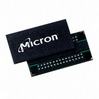
MT41J256M4HX-15E:D TR Micron Technology Inc, MT41J256M4HX-15E:D TR Datasheet - Page 128

MT41J256M4HX-15E:D TR
Manufacturer Part Number
MT41J256M4HX-15E:D TR
Description
IC DDR3 SDRAM 1GBIT 78FBGA
Manufacturer
Micron Technology Inc
Type
DDR3 SDRAMr
Specifications of MT41J256M4HX-15E:D TR
Format - Memory
RAM
Memory Type
DDR3 SDRAM
Memory Size
1G (256M x 4)
Speed
667MHz
Interface
Parallel
Voltage - Supply
1.425 V ~ 1.575 V
Operating Temperature
0°C ~ 95°C
Package / Case
78-FBGA
Organization
256Mx4
Density
1Gb
Address Bus
17b
Maximum Clock Rate
1.333GHz
Operating Supply Voltage (typ)
1.5V
Package Type
FBGA
Operating Temp Range
0C to 95C
Operating Supply Voltage (max)
1.575V
Operating Supply Voltage (min)
1.425V
Supply Current
220mA
Pin Count
78
Mounting
Surface Mount
Operating Temperature Classification
Commercial
Lead Free Status / RoHS Status
Lead free / RoHS Compliant
- Current page: 128 of 181
- Download datasheet (9Mb)
Figure 67: Example: Meeting
Figure 68: Example:
PDF: 09005aef826aa906/Source: 09005aef82a357c3
1Gb_DDR3_4.fm - Rev. F 11/08 EN
Command
Command
Address
BA[2:0]
Address
BA[2:0]
CK#
CK
CK#
CK
Bank x
Row
ACT
Bank a
T0
Row
ACT
T0
NOP
t RRD
T1
NOP
T1
t
FAW
the next whole number to determine the earliest clock edge after the ACTIVATE
command on which a READ or WRITE command can be entered. The same procedure is
used to convert other specification limits from time units to clock cycles.
When at least one bank is open, any READ-to-READ command delay or WRITE-to-
WRITE command delay is restricted to
A subsequent ACTIVATE command to a different row in the same bank can only be
issued after the previous active row has been closed (precharged). The minimum time
interval between successive ACTIVATE commands to the same bank is defined by
A subsequent ACTIVATE command to another bank can be issued while the first bank is
being accessed, which results in a reduction of total row-access overhead. The minimum
time interval between successive ACTIVATE commands to different banks is defined by
t
t
eter applies, regardless of the number of banks already opened or closed.
RRD. No more than four bank ACTIVATE commands may be issued in a given
FAW (MIN) period, and the
t RRD
Bank b
NOP
T2
Row
ACT
T4
t
RRD (MIN) and
Bank y
Row
ACT
NOP
T3
T5
t
RCD (MIN)
NOP
Bank c
t
T4
Row
T8
ACT
RRD (MIN) restriction still applies. The
128
t FAW
NOP
NOP
T5
T9
t
Micron Technology, Inc., reserves the right to change products or specifications without notice.
CCD (MIN).
t RCD
Bank d
1Gb: x4, x8, x16 DDR3 SDRAM
NOP
ACT
Row
T10
T8
NOP
NOP
Indicates A Break in
Time Scale
T11
T9
Indicates A Break in
Time Scale
©2006 Micron Technology, Inc. All rights reserved.
t
FAW (MIN) param-
NOP
NOP
T10
T19
Operations
Bank e
RD/WR
Bank y
Bank y
Bank y
T20
Row
Don’t Care
ACT
Don’t Care
T11
Col
t
RC.
Related parts for MT41J256M4HX-15E:D TR
Image
Part Number
Description
Manufacturer
Datasheet
Request
R

Part Number:
Description:
Manufacturer:
Micron Technology Inc
Datasheet:

Part Number:
Description:
Manufacturer:
Micron Technology Inc
Datasheet:

Part Number:
Description:
IC SDRAM 64MBIT 133MHZ 54TSOP
Manufacturer:
Micron Technology Inc
Datasheet:

Part Number:
Description:
IC SDRAM 64MBIT 5.5NS 86TSOP
Manufacturer:
Micron Technology Inc
Datasheet:

Part Number:
Description:
IC SDRAM 64MBIT 200MHZ 86TSOP
Manufacturer:
Micron Technology Inc
Datasheet:

Part Number:
Description:
IC SDRAM 64MBIT 133MHZ 54TSOP
Manufacturer:
Micron Technology Inc
Datasheet:

Part Number:
Description:
IC SDRAM 128MBIT 133MHZ 54TSOP
Manufacturer:
Micron Technology Inc
Datasheet:

Part Number:
Description:
IC SDRAM 256MBIT 133MHZ 90VFBGA
Manufacturer:
Micron Technology Inc
Datasheet:

Part Number:
Description:
IC SDRAM 128MBIT 133MHZ 54TSOP
Manufacturer:
Micron Technology Inc
Datasheet:

Part Number:
Description:
IC SDRAM 256MBIT 133MHZ 54TSOP
Manufacturer:
Micron Technology Inc
Datasheet:

Part Number:
Description:
IC DDR SDRAM 512MBIT 6NS 66TSOP
Manufacturer:
Micron Technology Inc
Datasheet:

Part Number:
Description:
IC SDRAM 128MBIT 167MHZ 86TSOP
Manufacturer:
Micron Technology Inc
Datasheet:

Part Number:
Description:
IC SDRAM 128MBIT 143MHZ 86TSOP
Manufacturer:
Micron Technology Inc
Datasheet:

Part Number:
Description:
SDRAM 256M-BIT 1.8V 54-PIN VFBGA
Manufacturer:
Micron Technology Inc
Datasheet:

Part Number:
Description:
IC SDRAM 128MBIT 143MHZ 86TSOP
Manufacturer:
Micron Technology Inc
Datasheet:


