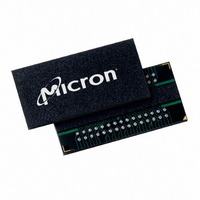
MT41J256M4HX-15E:D TR Micron Technology Inc, MT41J256M4HX-15E:D TR Datasheet - Page 31

MT41J256M4HX-15E:D TR
Manufacturer Part Number
MT41J256M4HX-15E:D TR
Description
IC DDR3 SDRAM 1GBIT 78FBGA
Manufacturer
Micron Technology Inc
Type
DDR3 SDRAMr
Specifications of MT41J256M4HX-15E:D TR
Format - Memory
RAM
Memory Type
DDR3 SDRAM
Memory Size
1G (256M x 4)
Speed
667MHz
Interface
Parallel
Voltage - Supply
1.425 V ~ 1.575 V
Operating Temperature
0°C ~ 95°C
Package / Case
78-FBGA
Organization
256Mx4
Density
1Gb
Address Bus
17b
Maximum Clock Rate
1.333GHz
Operating Supply Voltage (typ)
1.5V
Package Type
FBGA
Operating Temp Range
0C to 95C
Operating Supply Voltage (max)
1.575V
Operating Supply Voltage (min)
1.425V
Supply Current
220mA
Pin Count
78
Mounting
Surface Mount
Operating Temperature Classification
Commercial
Lead Free Status / RoHS Status
Lead free / RoHS Compliant
- Current page: 31 of 181
- Download datasheet (9Mb)
Table 13:
PDF: 09005aef826aa906/Source: 09005aef82a357c3
1Gb_DDR3_D2.fm - Rev. F 11/08 EN
I
Timing example
CKE
External clock
t
t
t
t
t
t
CL
AL
CS#
Command inputs
Row/column addresses
Bank addresses
Data I/O
Output buffer DQ, DQS
ODT
Burst length
Active banks
Idle banks
Special notes
DD
CK
RC
RAS
RCD
RRD
RC
Test
I
DD
Measurement Conditions for I
Notes:
Address input A10 must be LOW at all times
HIGH between ACTIVATE and PRECHARGE
ACTIVATE and PRECHARGE commands;
One Bank ACTIVATE to PRECHARGE
Bank 0; ACTIVATE-to-PRECHARGE loop
1. For further definition of input switching, see Table 10 on page 29.
2. For further definition of data switching, see Table 11 on page 29.
Switching—the only exceptions are
Example of -25E I
Bank address is fixed (bank 0)
I
DD
A0DDDDDDDDDDDDDDP0
Row addresses switching;
0: Operating Current 0
Electrical Specifications – I
t
t
t
RAS (MIN) I
CK (MIN) I
RC (MIN) I
Switching
Disabled
All other
HIGH
n/a
n/a
n/a
n/a
n/a
Off
n/a
n/a
On
–
DD
DD
DD
DD
0 pattern:
DD
0 and I
31
DD
1
Micron Technology, Inc., reserves the right to change products or specifications without notice.
Address input A10 must be LOW at all times
data is stable during falling DQS; I/O should
Bank 0; ACTIVATE-to-READ-to-PRECHARGE
every clock cycle, which means that read
ACTIVATE and PRECHARGE commands;
Read data: Output data switches after
HIGH between ACTIVATE, READ, and
Switching—the only exceptions are
DD
One Bank ACTIVATE to READ
be floating when no read data
Example of -25E I
Bank address is fixed (bank 0)
I
A0DDDDR0DDDDDDDDDP0
DD
Row addresses switching;
1Gb: x4, x8, x16 DDR3 SDRAM
Specifications and Conditions
1: Operating Current 1
Figure 14 on page 32
8 fixed (via MR0)
to PRECHARGE
t
t
t
RCD (MIN) I
t
RAS (MIN) I
PRECHARGE
CK (MIN) I
RC (MIN) I
Disabled
All other
CL I
HIGH
loop
Off
n/a
n/a
n/a
On
0
DD
DD
©2006 Micron Technology, Inc. All rights reserved.
DD
DD
DD
DD
1 pattern:
Notes
1
1
2
Related parts for MT41J256M4HX-15E:D TR
Image
Part Number
Description
Manufacturer
Datasheet
Request
R

Part Number:
Description:
Manufacturer:
Micron Technology Inc
Datasheet:

Part Number:
Description:
Manufacturer:
Micron Technology Inc
Datasheet:

Part Number:
Description:
IC SDRAM 64MBIT 133MHZ 54TSOP
Manufacturer:
Micron Technology Inc
Datasheet:

Part Number:
Description:
IC SDRAM 64MBIT 5.5NS 86TSOP
Manufacturer:
Micron Technology Inc
Datasheet:

Part Number:
Description:
IC SDRAM 64MBIT 200MHZ 86TSOP
Manufacturer:
Micron Technology Inc
Datasheet:

Part Number:
Description:
IC SDRAM 64MBIT 133MHZ 54TSOP
Manufacturer:
Micron Technology Inc
Datasheet:

Part Number:
Description:
IC SDRAM 128MBIT 133MHZ 54TSOP
Manufacturer:
Micron Technology Inc
Datasheet:

Part Number:
Description:
IC SDRAM 256MBIT 133MHZ 90VFBGA
Manufacturer:
Micron Technology Inc
Datasheet:

Part Number:
Description:
IC SDRAM 128MBIT 133MHZ 54TSOP
Manufacturer:
Micron Technology Inc
Datasheet:

Part Number:
Description:
IC SDRAM 256MBIT 133MHZ 54TSOP
Manufacturer:
Micron Technology Inc
Datasheet:

Part Number:
Description:
IC DDR SDRAM 512MBIT 6NS 66TSOP
Manufacturer:
Micron Technology Inc
Datasheet:

Part Number:
Description:
IC SDRAM 128MBIT 167MHZ 86TSOP
Manufacturer:
Micron Technology Inc
Datasheet:

Part Number:
Description:
IC SDRAM 128MBIT 143MHZ 86TSOP
Manufacturer:
Micron Technology Inc
Datasheet:

Part Number:
Description:
SDRAM 256M-BIT 1.8V 54-PIN VFBGA
Manufacturer:
Micron Technology Inc
Datasheet:

Part Number:
Description:
IC SDRAM 128MBIT 143MHZ 86TSOP
Manufacturer:
Micron Technology Inc
Datasheet:


