C8051F360DK Silicon Laboratories Inc, C8051F360DK Datasheet - Page 131
C8051F360DK
Manufacturer Part Number
C8051F360DK
Description
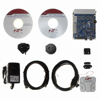
KIT DEV FOR C8051F360 FAMILY
Manufacturer
Silicon Laboratories Inc
Type
MCUr
Specifications of C8051F360DK
Contents
Evaluation Board, Power Supply, USB Cables, Adapter and Documentation
Processor To Be Evaluated
C8051F36x
Interface Type
USB
Lead Free Status / RoHS Status
Lead free / RoHS Compliant
For Use With/related Products
C8051F360, F361, F362, F363, F364, F365, F366, F367, F368, F369
Lead Free Status / Rohs Status
Lead free / RoHS Compliant
Other names
336-1410


12.3. External Reset
The external RST pin provides a means for external circuitry to force the device into a reset state. Assert-
ing an active-low signal on the RST pin generates a reset; an external pullup and/or decoupling of the RST
pin may be necessary to avoid erroneous noise-induced resets. See Table 12.1 for complete RST pin
specifications. The PINRSF flag (RSTSRC.0) is set on exit from an external reset.
12.4. Missing Clock Detector Reset
The Missing Clock Detector (MCD) is a one-shot circuit that is triggered by the system clock. If the system
clock remains high or low for more than 100 µs, the one-shot will time out and generate a reset. After a
MCD reset, the MCDRSF flag (RSTSRC.2) will read ‘1’, signifying the MCD as the reset source; otherwise,
this bit reads ‘0’. Writing a ‘1’ to the MCDRSF bit enables the Missing Clock Detector; writing a ‘0’ disables
it. The state of the RST pin is unaffected by this reset.
12.5. Comparator0 Reset
Comparator0 can be configured as a reset source by writing a ‘1’ to the C0RSEF flag (RSTSRC.5).
Comparator0 should be enabled and allowed to settle prior to writing to C0RSEF to prevent any turn-on
chatter on the output from generating an unwanted reset. The Comparator0 reset is active-low: if the non-
inverting input voltage (on CP0+) is less than the inverting input voltage (on CP0-), the device is put into
the reset state. After a Comparator0 reset, the C0RSEF flag (RSTSRC.5) will read ‘1’ signifying
Comparator0 as the reset source; otherwise, this bit reads ‘0’. The state of the RST pin is unaffected by
this reset.
Bit 7:
Bit 6:
Bits 5–0: RESERVED. Read = Variable. Write = don’t care.
SFR Page:
SFR Address:
VDMEN
R/W
Bit7
VDMEN: V
This bit turns the V
until it is also selected as a reset source in register RSTSRC (SFR Definition 12.2). The V
Monitor must be allowed to stabilize before it is selected as a reset source. Selecting the
V
0: V
1: V
V
This bit indicates the current power supply status (V
0: V
1: V
all pages
0xFF
DD
DD
VDDSTAT Reserved Reserved Reserved Reserved Reserved Reserved
DD
DD
DD
DD
Monitor as a reset source before it has stabilized may generate a system reset.
STAT: V
Bit6
R
Monitor Disabled.
Monitor Enabled.
is at or below the V
is above the V
SFR Definition 12.1. VDM0CN: V
DD
DD
Monitor Enable.
Status.
Bit5
R
DD
DD
Monitor circuit on/off. The V
Monitor threshold.
DD
Bit4
R
Monitor threshold.
C8051F360/1/2/3/4/5/6/7/8/9
Rev. 1.0
Bit3
R
DD
DD
Bit2
DD
R
Monitor cannot generate system resets
Monitor Control
Monitor output).
Bit1
R
Bit0
R
Reset Value
Variable
DD
131
Related parts for C8051F360DK
Image
Part Number
Description
Manufacturer
Datasheet
Request
R

Part Number:
Description:
SMD/C°/SINGLE-ENDED OUTPUT SILICON OSCILLATOR
Manufacturer:
Silicon Laboratories Inc
Part Number:
Description:
Manufacturer:
Silicon Laboratories Inc
Datasheet:
Part Number:
Description:
N/A N/A/SI4010 AES KEYFOB DEMO WITH LCD RX
Manufacturer:
Silicon Laboratories Inc
Datasheet:
Part Number:
Description:
N/A N/A/SI4010 SIMPLIFIED KEY FOB DEMO WITH LED RX
Manufacturer:
Silicon Laboratories Inc
Datasheet:
Part Number:
Description:
N/A/-40 TO 85 OC/EZLINK MODULE; F930/4432 HIGH BAND (REV E/B1)
Manufacturer:
Silicon Laboratories Inc
Part Number:
Description:
EZLink Module; F930/4432 Low Band (rev e/B1)
Manufacturer:
Silicon Laboratories Inc
Part Number:
Description:
I°/4460 10 DBM RADIO TEST CARD 434 MHZ
Manufacturer:
Silicon Laboratories Inc
Part Number:
Description:
I°/4461 14 DBM RADIO TEST CARD 868 MHZ
Manufacturer:
Silicon Laboratories Inc
Part Number:
Description:
I°/4463 20 DBM RFSWITCH RADIO TEST CARD 460 MHZ
Manufacturer:
Silicon Laboratories Inc
Part Number:
Description:
I°/4463 20 DBM RADIO TEST CARD 868 MHZ
Manufacturer:
Silicon Laboratories Inc
Part Number:
Description:
I°/4463 27 DBM RADIO TEST CARD 868 MHZ
Manufacturer:
Silicon Laboratories Inc
Part Number:
Description:
I°/4463 SKYWORKS 30 DBM RADIO TEST CARD 915 MHZ
Manufacturer:
Silicon Laboratories Inc
Part Number:
Description:
N/A N/A/-40 TO 85 OC/4463 RFMD 30 DBM RADIO TEST CARD 915 MHZ
Manufacturer:
Silicon Laboratories Inc
Part Number:
Description:
I°/4463 20 DBM RADIO TEST CARD 169 MHZ
Manufacturer:
Silicon Laboratories Inc