C8051F360DK Silicon Laboratories Inc, C8051F360DK Datasheet - Page 190
C8051F360DK
Manufacturer Part Number
C8051F360DK
Description
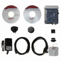
KIT DEV FOR C8051F360 FAMILY
Manufacturer
Silicon Laboratories Inc
Type
MCUr
Specifications of C8051F360DK
Contents
Evaluation Board, Power Supply, USB Cables, Adapter and Documentation
Processor To Be Evaluated
C8051F36x
Interface Type
USB
Lead Free Status / RoHS Status
Lead free / RoHS Compliant
For Use With/related Products
C8051F360, F361, F362, F363, F364, F365, F366, F367, F368, F369
Lead Free Status / Rohs Status
Lead free / RoHS Compliant
Other names
336-1410


C8051F360/1/2/3/4/5/6/7/8/9
17.3. General Purpose Port I/O
Port pins that remain unassigned by the Crossbar and are not used by analog peripherals can be used for
general purpose I/O. Ports P0-P3 are accessed through corresponding special function registers (SFRs)
that are both byte-addressable and bit-addressable. Port 4 (C8051F360/3 only) uses an SFR which is
byte-addressable. When writing to a Port, the value written to the SFR is latched to maintain the output
data value at each pin. When reading, the logic levels of the Port's input pins are returned regardless of the
XBRn settings (i.e., even when the pin is assigned to another signal by the Crossbar, the Port register can
always read its corresponding Port I/O pin). The exception to this is the execution of the read-modify-write
instructions that target a Port Latch register as the destination. The read-modify-write instructions when
operating on a Port SFR are the following: ANL, ORL, XRL, JBC, CPL, INC, DEC, DJNZ and MOV, CLR or
SETB, when the destination is an individual bit in a Port SFR. For these instructions, the value of the latch
register (not the pin) is read, modified, and written back to the SFR.
In addition to performing general purpose I/O, P0, P1, and P2 can generate a port match event if the logic
levels of the Port’s input pins match a software controlled value. A port match event is generated if
(P0 & P0MASK) does not equal (P0MATCH & P0MASK), if (P1 & P1MASK) does not equal
(P1MATCH & P1MASK), or if (P2 & P2MASK) does not equal (P2MATCH & P2MASK). This allows Soft-
ware to be notified if a certain change or pattern occurs on P0, P1, or P2 input pins regardless of the XBRn
settings. A port match event can cause an interrupt if EMAT (EIE2.1) is set to '1' or cause the internal oscil-
lator to awaken from SUSPEND mode. See Section “16.1.1. Internal Oscillator Suspend Mode” on
page 170 for more information.
190
Bits 7–0: P0.[7:0]
SFR Page:
SFR Address:
P0.7
R/W
Bit7
Write - Output appears on I/O pins per Crossbar Registers.
0: Logic Low Output.
1: Logic High Output (high impedance if corresponding P0MDOUT.n bit = 0).
Read - Always reads ‘0’ if selected as analog input in register P0MDIN. Directly reads Port
pin when configured as digital input.
0: P0.n pin is logic low.
1: P0.n pin is logic high.
all pages
0x80
P0.6
R/W
Bit6
P0.5
R/W
Bit5
(bit addressable)
SFR Definition 17.3. P0: Port0
P0.4
R/W
Bit4
Rev. 1.0
P0.3
R/W
Bit3
P0.2
R/W
Bit2
P0.1
R/W
Bit1
P0.0
R/W
Bit0
Reset Value
11111111
Related parts for C8051F360DK
Image
Part Number
Description
Manufacturer
Datasheet
Request
R

Part Number:
Description:
SMD/C°/SINGLE-ENDED OUTPUT SILICON OSCILLATOR
Manufacturer:
Silicon Laboratories Inc
Part Number:
Description:
Manufacturer:
Silicon Laboratories Inc
Datasheet:
Part Number:
Description:
N/A N/A/SI4010 AES KEYFOB DEMO WITH LCD RX
Manufacturer:
Silicon Laboratories Inc
Datasheet:
Part Number:
Description:
N/A N/A/SI4010 SIMPLIFIED KEY FOB DEMO WITH LED RX
Manufacturer:
Silicon Laboratories Inc
Datasheet:
Part Number:
Description:
N/A/-40 TO 85 OC/EZLINK MODULE; F930/4432 HIGH BAND (REV E/B1)
Manufacturer:
Silicon Laboratories Inc
Part Number:
Description:
EZLink Module; F930/4432 Low Band (rev e/B1)
Manufacturer:
Silicon Laboratories Inc
Part Number:
Description:
I°/4460 10 DBM RADIO TEST CARD 434 MHZ
Manufacturer:
Silicon Laboratories Inc
Part Number:
Description:
I°/4461 14 DBM RADIO TEST CARD 868 MHZ
Manufacturer:
Silicon Laboratories Inc
Part Number:
Description:
I°/4463 20 DBM RFSWITCH RADIO TEST CARD 460 MHZ
Manufacturer:
Silicon Laboratories Inc
Part Number:
Description:
I°/4463 20 DBM RADIO TEST CARD 868 MHZ
Manufacturer:
Silicon Laboratories Inc
Part Number:
Description:
I°/4463 27 DBM RADIO TEST CARD 868 MHZ
Manufacturer:
Silicon Laboratories Inc
Part Number:
Description:
I°/4463 SKYWORKS 30 DBM RADIO TEST CARD 915 MHZ
Manufacturer:
Silicon Laboratories Inc
Part Number:
Description:
N/A N/A/-40 TO 85 OC/4463 RFMD 30 DBM RADIO TEST CARD 915 MHZ
Manufacturer:
Silicon Laboratories Inc
Part Number:
Description:
I°/4463 20 DBM RADIO TEST CARD 169 MHZ
Manufacturer:
Silicon Laboratories Inc