C8051F360DK Silicon Laboratories Inc, C8051F360DK Datasheet - Page 181
C8051F360DK
Manufacturer Part Number
C8051F360DK
Description
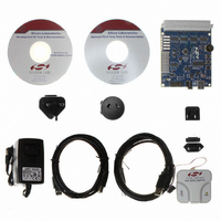
KIT DEV FOR C8051F360 FAMILY
Manufacturer
Silicon Laboratories Inc
Type
MCUr
Specifications of C8051F360DK
Contents
Evaluation Board, Power Supply, USB Cables, Adapter and Documentation
Processor To Be Evaluated
C8051F36x
Interface Type
USB
Lead Free Status / RoHS Status
Lead free / RoHS Compliant
For Use With/related Products
C8051F360, F361, F362, F363, F364, F365, F366, F367, F368, F369
Lead Free Status / Rohs Status
Lead free / RoHS Compliant
Other names
336-1410


Bits 7–0: PLLN7–0: PLL Multiplier.
SFR Page:
SFR Address:
Bits 7–6: UNUSED. Read = 00b. Write = don’t care.
Bits 5–4: PLLICO1-0: PLL Current-Controlled Oscillator Control Bits.
Bits 3–0: PLLLP3-0: PLL Loop Filter Control Bits.
SFR Page:
SFR Address:
PLLN7
R/W
Bit7
R/W
Bit7
–
These bits select the multiplication factor of the divided PLL reference clock. When set to
any non-zero value, the multiplication factor will be equal to the value in PLLN7-0. When set
to ‘00000000b’, the multiplication factor will be equal to 256.
Selection is based on the desired output frequency, according to the following table:
Selection is based on the divided PLL reference clock, according to the following table:
All other states of PLLLP3–0 are RESERVED.
F
0xB1
F
0xB2
PLLN6
Divided PLL Reference Clock
R/W
Bit6
R/W
Bit6
–
SFR Definition 16.8. PLL0MUL: PLL Clock Scaler
PLL Output Clock
12.2–19.5 MHz
7.8–12.5 MHz
65–100 MHz
PLLICO1 PLLICO0
45–80 MHz
30–60 MHz
25–50 MHz
19–30 MHz
PLLN5
SFR Definition 16.9. PLL0FLT: PLL Filter
5–8 MHz
R/W
Bit5
R/W
Bit5
PLLN4
R/W
Bit4
R/W
Bit4
C8051F360/1/2/3/4/5/6/7/8/9
Rev. 1.0
PLLLP3
PLLN3
R/W
Bit3
R/W
Bit3
PLLLP2
PLLN2
R/W
Bit2
R/W
Bit2
PLLICO1-0
PLLLP3-0
0001
0011
0111
1111
00
01
10
11
PLLLP1
PLLN1
R/W
Bit1
R/W
Bit1
PLLLP0 00110001
PLLN0
R/W
Bit0
R/W
Bit0
00000001
Reset Value
Reset Value
181
Related parts for C8051F360DK
Image
Part Number
Description
Manufacturer
Datasheet
Request
R

Part Number:
Description:
SMD/C°/SINGLE-ENDED OUTPUT SILICON OSCILLATOR
Manufacturer:
Silicon Laboratories Inc
Part Number:
Description:
Manufacturer:
Silicon Laboratories Inc
Datasheet:
Part Number:
Description:
N/A N/A/SI4010 AES KEYFOB DEMO WITH LCD RX
Manufacturer:
Silicon Laboratories Inc
Datasheet:
Part Number:
Description:
N/A N/A/SI4010 SIMPLIFIED KEY FOB DEMO WITH LED RX
Manufacturer:
Silicon Laboratories Inc
Datasheet:
Part Number:
Description:
N/A/-40 TO 85 OC/EZLINK MODULE; F930/4432 HIGH BAND (REV E/B1)
Manufacturer:
Silicon Laboratories Inc
Part Number:
Description:
EZLink Module; F930/4432 Low Band (rev e/B1)
Manufacturer:
Silicon Laboratories Inc
Part Number:
Description:
I°/4460 10 DBM RADIO TEST CARD 434 MHZ
Manufacturer:
Silicon Laboratories Inc
Part Number:
Description:
I°/4461 14 DBM RADIO TEST CARD 868 MHZ
Manufacturer:
Silicon Laboratories Inc
Part Number:
Description:
I°/4463 20 DBM RFSWITCH RADIO TEST CARD 460 MHZ
Manufacturer:
Silicon Laboratories Inc
Part Number:
Description:
I°/4463 20 DBM RADIO TEST CARD 868 MHZ
Manufacturer:
Silicon Laboratories Inc
Part Number:
Description:
I°/4463 27 DBM RADIO TEST CARD 868 MHZ
Manufacturer:
Silicon Laboratories Inc
Part Number:
Description:
I°/4463 SKYWORKS 30 DBM RADIO TEST CARD 915 MHZ
Manufacturer:
Silicon Laboratories Inc
Part Number:
Description:
N/A N/A/-40 TO 85 OC/4463 RFMD 30 DBM RADIO TEST CARD 915 MHZ
Manufacturer:
Silicon Laboratories Inc
Part Number:
Description:
I°/4463 20 DBM RADIO TEST CARD 169 MHZ
Manufacturer:
Silicon Laboratories Inc