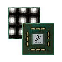
MPC8536DS Freescale Semiconductor, MPC8536DS Datasheet - Page 103

MPC8536DS
Manufacturer Part Number
MPC8536DS
Description
BOARD DEV SYSTEM MPC8536E
Manufacturer
Freescale Semiconductor
Series
PowerQUICC III™r
Type
MPUr
Datasheets
1.MPC8536EBVTAVLA.pdf
(127 pages)
2.MPC8536EBVTAVLA.pdf
(1706 pages)
3.MPC8536DS.pdf
(2 pages)
4.MPC8536DS.pdf
(126 pages)
Specifications of MPC8536DS
Contents
Board, Software and Documentation
Processor Series
MPC85xx
Core
e500
Data Bus Width
32 bit
Maximum Clock Frequency
667 MHz
Operating Supply Voltage
- 0.3 V to + 1.21 V
Maximum Operating Temperature
+ 105 C
Data Ram Size
32 KB
Interface Type
SPI, USB
Program Memory Type
DDR2, DDR3, SDRAM
Core Size
32 Bit
Program Memory Size
544KB
Cpu Speed
1.5GHz
Digital Ic Case Style
BGA
No. Of Pins
783
Supply Voltage Range
0.95V To 1.05V
Rohs Compliant
Yes
For Use With/related Products
MPC8536
Lead Free Status / RoHS Status
Lead free / RoHS Compliant
2.21.4.2
The TX eye diagram in
any real PCI Express interconnect + RX component.
There are two eye diagrams that must be met for the transmitter. Both eye diagrams must be aligned in time using the jitter
median to locate the center of the eye diagram. The different eye diagrams will differ in voltage depending whether it is a
transition bit or a de-emphasized bit. The exact reduced voltage level of the de-emphasized bit will always be relative to the
transition bit.
The eye diagram must be valid for any 250 consecutive UIs.
A recovered TX UI is calculated over 3500 consecutive unit intervals of sample data. The eye diagram is created using all edges
of the 250 consecutive UI in the center of the 3500 UI used for calculating the TX UI.
2.21.4.3
Table 72
component pins.
UI
V
RX-DIFFp-p
Symbol
defines the specifications for the differential input at all receivers (RXs). The parameters are specified at the
Figure 69. Minimum Transmitter Timing and Voltage Output Compliance Specifications
Transmitter Compliance Eye Diagrams
Differential Receiver (RX) Input Specifications
It is recommended that the recovered TX UI is calculated using all edges in the 3500
consecutive UI interval with a fit algorithm using a minimization merit function (that is,
least squares and median deviation fits).
Unit Interval
Differential
Peak-to-Peak
Output Voltage
Figure 69
Parameter
Table 72. Differential Receiver (RX) Input Specifications
is specified using the passive compliance/test measurement load (see
399.8
0.175
Min
8
Nom
400
—
NOTE
400.12
1.200
Max
Units
ps
V
Each UI is 400 ps ± 300 ppm. UI does not
account for Spread Spectrum Clock dictated
variations. See Note 1.
V
See Note 2.
RX-DIFFp-p
= 2*|V
Comments
RX-D+
Figure
– V
RX-D-
71) in place of
|


