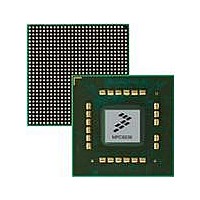
MPC8536DS Freescale Semiconductor, MPC8536DS Datasheet - Page 39

MPC8536DS
Manufacturer Part Number
MPC8536DS
Description
BOARD DEV SYSTEM MPC8536E
Manufacturer
Freescale Semiconductor
Series
PowerQUICC III™r
Type
MPUr
Datasheets
1.MPC8536EBVTAVLA.pdf
(127 pages)
2.MPC8536EBVTAVLA.pdf
(1706 pages)
3.MPC8536DS.pdf
(2 pages)
4.MPC8536DS.pdf
(126 pages)
Specifications of MPC8536DS
Contents
Board, Software and Documentation
Processor Series
MPC85xx
Core
e500
Data Bus Width
32 bit
Maximum Clock Frequency
667 MHz
Operating Supply Voltage
- 0.3 V to + 1.21 V
Maximum Operating Temperature
+ 105 C
Data Ram Size
32 KB
Interface Type
SPI, USB
Program Memory Type
DDR2, DDR3, SDRAM
Core Size
32 Bit
Program Memory Size
544KB
Cpu Speed
1.5GHz
Digital Ic Case Style
BGA
No. Of Pins
783
Supply Voltage Range
0.95V To 1.05V
Rohs Compliant
Yes
For Use With/related Products
MPC8536
Lead Free Status / RoHS Status
Lead free / RoHS Compliant
Figure 12
Figure 13
the clock, these AC timing diagrams also apply when the falling edge is the active edge.
Figure 13
Freescale Semiconductor
SPI_CS outputs—Master data delay
SPI inputs—Master data input setup time
SPI inputs—Master data input hold time
Notes:
1. Output specifications are measured from the 50% level of the rising edge of CLKIN to the 50% level of the signal.
2. The symbols used for timing specifications follow the pattern of t
3. SPCOM[RxDelay] is set to 0.
4. SPCOM[RxDelay] is set to 1.
SPICLK (output)
Timings are measured at the pin.
(reference)(state)
t
the high state (H) until outputs (O) are valid (V).
NIKHOV
Output Signals:
Output Signals:
provides the AC test load for the SPI.
represent the AC timing from
shows the SPI timing in Master mode (internal clock).
Input Signals:
SPI_CS[0:3]
(See Note)
Note: The clock edge is selectable on SPI.
(See Note)
(See Note)
SPIMISO
SPIMOSI
symbolizes the NMSI outputs internal timing (NI) for the time t
MPC8536E PowerQUICC III Integrated Processor Hardware Specifications, Rev. 3
for inputs and t
Characteristic
Figure 13. SPI AC Timing in Master mode (Internal Clock) Diagram
Output
Table 21. SPI AC Timing Specifications
(first two letters of functional block)(reference)(state)(signal)(state)
Table
t
NIIVKH
Figure 12. SPI AC Test Load
21. Note that although the specifications generally reference the rising edge of
t
Z
t
NIKHOV2
NIKHOV
0
= 50 Ω
t
NIIXKH
Symbol
t
NIKHOV2
t
t
NIIVKH
NIIXKH
2
(first two letters of functional block)(signal)(state)
R
SPI
L
Min
1
—
5
0
= 50 Ω
(continued)
memory clock reference (K) goes from
Max
for outputs. For example,
OV
6.0
—
—
t
NIKHOX2
DD
t
NIKHOX
/2
Unit
ns
ns
ns
Note
—
—
—
eSPI
39


