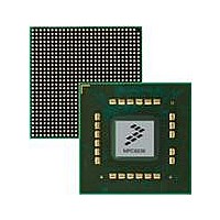
MPC8536DS Freescale Semiconductor, MPC8536DS Datasheet - Page 116

MPC8536DS
Manufacturer Part Number
MPC8536DS
Description
BOARD DEV SYSTEM MPC8536E
Manufacturer
Freescale Semiconductor
Series
PowerQUICC III™r
Type
MPUr
Datasheets
1.MPC8536EBVTAVLA.pdf
(127 pages)
2.MPC8536EBVTAVLA.pdf
(1706 pages)
3.MPC8536DS.pdf
(2 pages)
4.MPC8536DS.pdf
(126 pages)
Specifications of MPC8536DS
Contents
Board, Software and Documentation
Processor Series
MPC85xx
Core
e500
Data Bus Width
32 bit
Maximum Clock Frequency
667 MHz
Operating Supply Voltage
- 0.3 V to + 1.21 V
Maximum Operating Temperature
+ 105 C
Data Ram Size
32 KB
Interface Type
SPI, USB
Program Memory Type
DDR2, DDR3, SDRAM
Core Size
32 Bit
Program Memory Size
544KB
Cpu Speed
1.5GHz
Digital Ic Case Style
BGA
No. Of Pins
783
Supply Voltage Range
0.95V To 1.05V
Rohs Compliant
Yes
For Use With/related Products
MPC8536
Lead Free Status / RoHS Status
Lead free / RoHS Compliant
SerDes Block Power Supply Decoupling Recommendations
These capacitors should have a value of 0.1 µF. Only ceramic SMT (surface mount technology) capacitors should be used to
minimize lead inductance, preferably 0402 or 0603 sizes.
In addition, it is recommended that there be several bulk storage capacitors distributed around the PCB, feeding the V
BV
have a low ESR (equivalent series resistance) rating to ensure the quick response time necessary. They should also be connected
to the power and ground planes through two vias to minimize inductance. Suggested bulk capacitors—100–330 µF (AVX TPS
tantalum or Sanyo OSCON). However, customers should work directly with their power regulator vendor for best values types
and quantity of bulk capacitors.
3.5
he SerDes1 and SerDes2 blocks require a clean, tightly regulated source of power (SnV
transmit and reliable recovery of data in the receiver. An appropriate decoupling scheme is outlined below.
Only surface mount technology (SMT) capacitors should be used to minimize inductance. Connections from all capacitors to
power and ground should be done with multiple vias to further reduce inductance.
3.6
To ensure reliable operation, it is highly recommended to connect unused inputs to an appropriate signal level. All unused active
low inputs should be tied to V
connected to GND. All NC (no-connect) signals must remain unconnected. Power and ground connections must be made to all
external V
3.7
The MPC8536E requires weak pull-up resistors (2–10 kΩ is recommended) on open drain type pins including I
MPIC interrupt pins.
Correct operation of the JTAG interface requires configuration of a group of system control pins as demonstrated in
Care must be taken to ensure that these pins are maintained at a valid deasserted state under normal operating conditions as most
have asynchronous behavior and spurious assertion will give unpredictable results.
The following pins must NOT be pulled down during power-on reset: TSEC1_TXD[3], HRESET_REQ,
TRIG_OUT/READY/QUIESCE, MSRCID[2:4], ASLEEP. The UART_SOUT[0:1] and TEST_SEL pins must be set to a
proper state during POR configuration. Please refer to the pinlist table (see
See the PCI 2.2 specification for all pull-ups required for PCI.
3.8
The MPC8536E drivers are characterized over process, voltage, and temperature. For all buses, the driver is a push-pull
single-ended driver type (open drain for I
116
DD
•
•
•
, OV
First, the board should have at least 10 x 10-nF SMT ceramic chip capacitors as close as possible to the supply balls
of the device. Where the board has blind vias, these capacitors should be placed directly below the chip supply and
ground connections. Where the board does not have blind vias, these capacitors should be placed in a ring around the
device as close to the supply and ground connections as possible.
Second, there should be a 1-µF ceramic chip capacitor from each SerDes supply (SnV
ground plane on each side of the device. This should be done for all SerDes supplies.
Third, between the device and any SerDes voltage regulator there should be a 10-µF, low equivalent series resistance
(ESR) SMT tantalum chip capacitor and a 100-µF, low ESR SMT tantalum chip capacitor. This should be done for all
SerDes supplies.
DD,
DD
SerDes Block Power Supply Decoupling Recommendations
Connection Recommendations
Pull-Up and Pull-Down Resistor Requirements
Output Buffer DC Impedance
TV
, GV
DD
DD
, BV
MPC8536E PowerQUICC III Integrated Processor Hardware Specifications, Rev. 3
, and LV
DD
, OV
DD
DD,
DD
planes, to enable quick recharging of the smaller chip capacitors. These bulk capacitors should
TV
, GV
DD
, BV
DD
2
C).
, and LV
DD
, OV
DD
DD
, GV
and GND pins of the device.
DD
, and LV
DD
as required. All unused active high inputs should be
Table
62) of the individual device for more details.
DD
and XnV
DD
and XnV
DD
Freescale Semiconductor
) to ensure low jitter on
DD
) to the board
2
C pins and
DD
Figure
, TV
DD
78.
,


