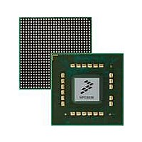
MPC8536DS Freescale Semiconductor, MPC8536DS Datasheet - Page 25

MPC8536DS
Manufacturer Part Number
MPC8536DS
Description
BOARD DEV SYSTEM MPC8536E
Manufacturer
Freescale Semiconductor
Series
PowerQUICC III™r
Type
MPUr
Datasheets
1.MPC8536EBVTAVLA.pdf
(127 pages)
2.MPC8536EBVTAVLA.pdf
(1706 pages)
3.MPC8536DS.pdf
(2 pages)
4.MPC8536DS.pdf
(126 pages)
Specifications of MPC8536DS
Contents
Board, Software and Documentation
Processor Series
MPC85xx
Core
e500
Data Bus Width
32 bit
Maximum Clock Frequency
667 MHz
Operating Supply Voltage
- 0.3 V to + 1.21 V
Maximum Operating Temperature
+ 105 C
Data Ram Size
32 KB
Interface Type
SPI, USB
Program Memory Type
DDR2, DDR3, SDRAM
Core Size
32 Bit
Program Memory Size
544KB
Cpu Speed
1.5GHz
Digital Ic Case Style
BGA
No. Of Pins
783
Supply Voltage Range
0.95V To 1.05V
Rohs Compliant
Yes
For Use With/related Products
MPC8536
Lead Free Status / RoHS Status
Lead free / RoHS Compliant
2.1.3
Table 3
2.2
The MPC8536E requires its power rails to be applied in a specific sequence in order to ensure proper device operation. These
requirements are as follows for power up:
All supplies must be at their stable values within 50 ms.
Items on the same line have no ordering requirement with respect to one another. Items on separate lines must be ordered
sequentially such that voltage rails on a previous step must reach 90% of their value before the voltage rails on the current step
reach 10% of theirs.
In order to guarantee MCKE low during power-up, the above sequencing for GV
of the DDR signals being in an indeterminate state during power-up, then the sequencing for GV
From a system standpoint, if any of the I/O power supplies ramp prior to the VDD platform supply, the I/Os associated with
that I/O supply may drive a logic one or zero during power-up, and extra current may be drawn by the device.
During the Deep Sleep state, the VDD core supply is removed. But all other power supplies remain applied. Therefore, there is
no requirement to apply the VDD core supply before any other power rails when the silicon waking from Deep Sleep.
Freescale Semiconductor
Local bus interface utilities signals
PCI signals
DDR2 signal
DDR3 signal
TSEC signals
DUART, system control, JTAG
I
Notes:
1. The drive strength of the local bus interface is determined by the configuration of the appropriate bits in PORIMPSCR.
2. The drive strength of the PCI interface is determined by the setting of the PCI1_GNT1 signal at reset.
3. The drive strength of the DDR2 or DDR3 interface in half-strength mode is at T
2
C
1.
2.
3.
provides information on the characteristics of the output driver strengths. The values are preliminary estimates.
V
SV
[Wait for POWER_EN to assert], then V
GV
DD_PLAT
Power Sequencing
DD
DD
Output Driver Characteristics
,S2V
, V
MPC8536E PowerQUICC III Integrated Processor Hardware Specifications, Rev. 3
DD
DD_CORE
Driver Type
, TV
DD
, XV
(if POWER_EN is not used to control V
DD
and X2V
Table 4. Output Drive Capability
DD
DD_CORE
(if POWER_EN is used to control V
32 (half strength mode)
40 (half strength mode)
Output Impedance
Programmable
42 (default)
45(default)
45(default)
125
150
DD_CORE
(Ω)
25
35
25
16
20
42
42
DD
), AV
j
is required. If there is no concern about any
= 105°C and at GV
DD
, BV
LV
DD
DD_CORE
GV
GV
BV
BV
BV
BV
BV
OV
OV
OV
DD
DD
, LV
Voltage
Supply
DD
DD
DD
DD
DD
DD
DD
DD
DD
DD
is not required.
= 2.5/3.3 V
DD
DD
= 3.3 V
= 2.5 V
= 3.3 V
= 2.5 V
= 1.8 V
= 3.3 V
= 1.8 V
= 1.5 V
= 3.3 V
= 3.3 V
, OV
)
(min)
Power Sequencing
DD
,
Notes
—
—
—
1
2
3
2
25


